

ABO3/MgO/GaN heterojunction structure and preparation method thereof
A heterogeneous structure and thin film technology, applied in the field of microelectronic materials, to achieve the effects of reducing device power consumption, protection performance, and reducing gate leakage current
- Summary
- Abstract
- Description
- Claims
- Application Information
AI Technical Summary
Problems solved by technology
Method used
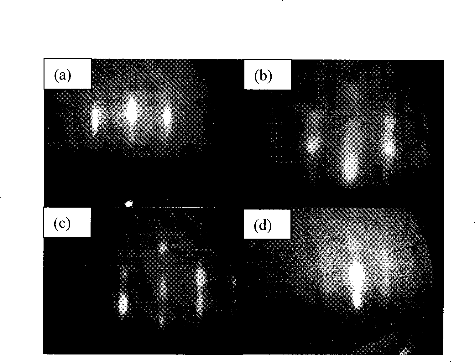
Image

Examples
Embodiment Construction
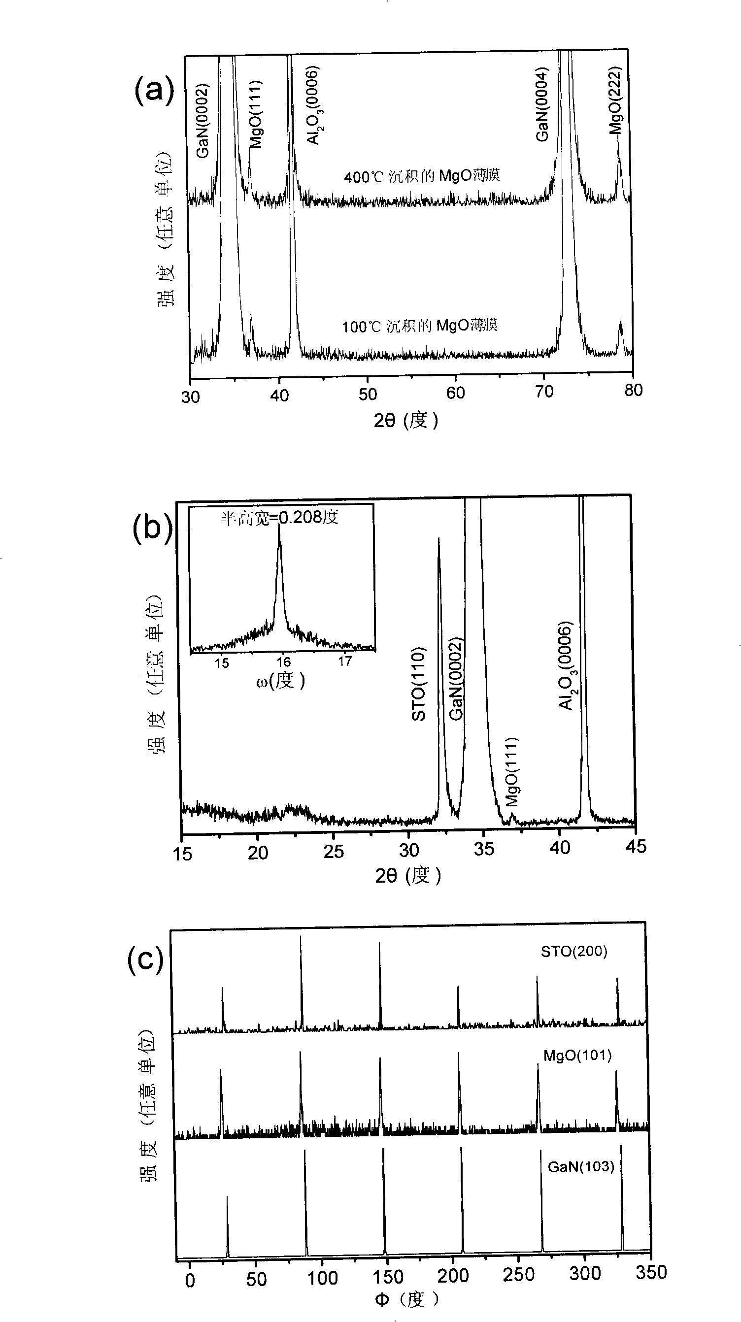
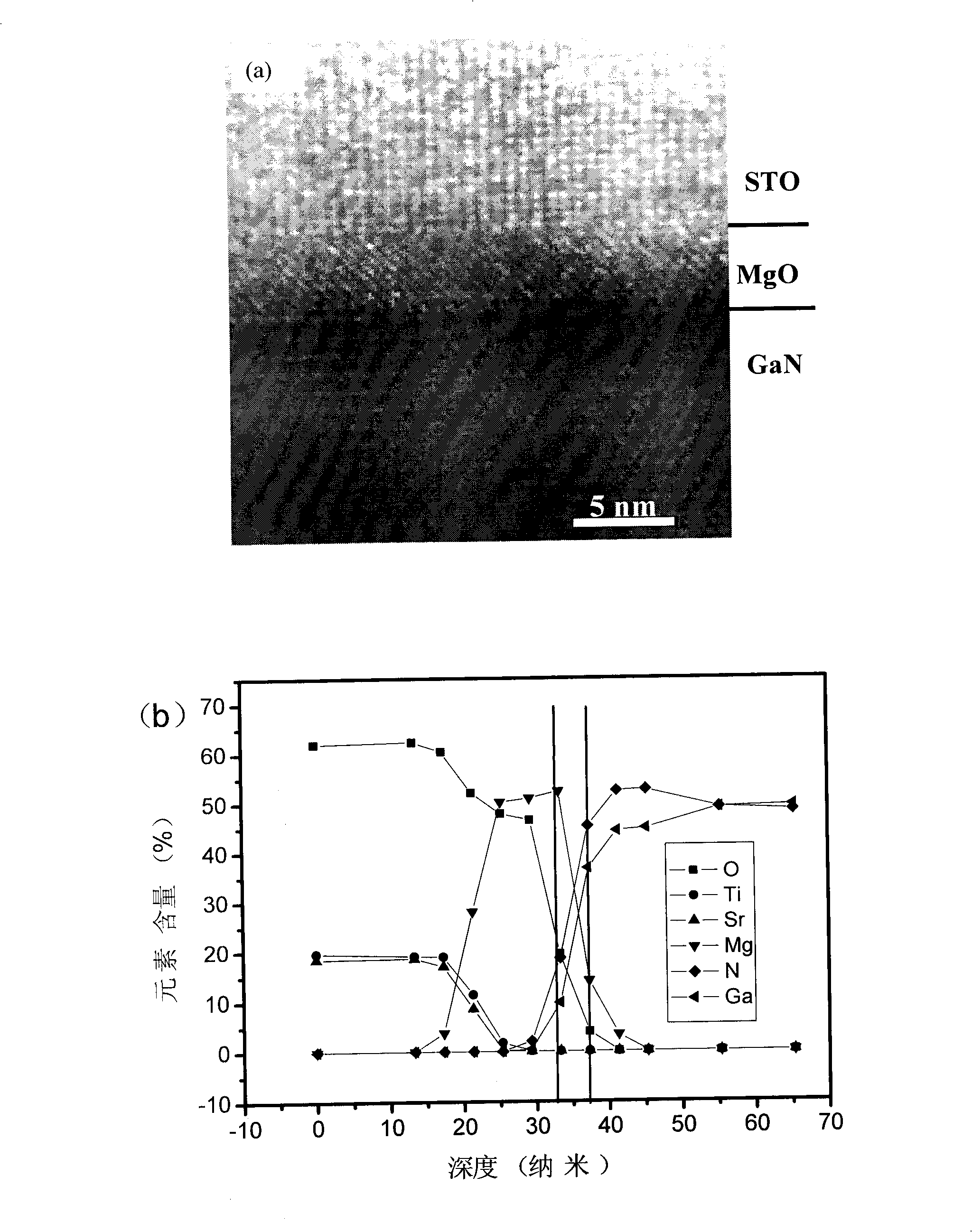
[0034] ABO of this embodiment 3 / MgO / GaN heterostructure has three layers, on the substrate substrate and ABO 3 Between, there is a MgO nano-buffer layer thin film, and the substrate substrate is GaN or GaN covered with 20nm AlGaN.
[0035] Further, GaN or AlGaN is oriented in the (0001) direction. MgO films are oriented along the (111) direction. ABOs 3 In the metal oxide, A is an element of Mg, Ca, Sr, Ba, Pb, Bi, La, and B is an element of Ti, Zr, Fe, Ru, Ni;
[0036] A can also be a solid solution composed of two or more elements in Mg, Ca, Sr, Ba, Pb, Bi, La, and B is two or more elements in Ti, Zr, Fe, Ru, Ni The solid solution constituted, and, based on the molar ratio of A element, B element and oxygen element, the stoichiometric ratio satisfies (A 1 +A 2 +...+An): (B 1 +B 2 +...+Bn):O=1:1:3.
[0037] The ABO 3 Metal oxides can be doped with a certain proportion of modified oxides, namely RE A oxide or RE B oxides, the stoichiometric ratio satisfies (A 1 +...
PUM
 Abstract
Description
Claims
Application Information