

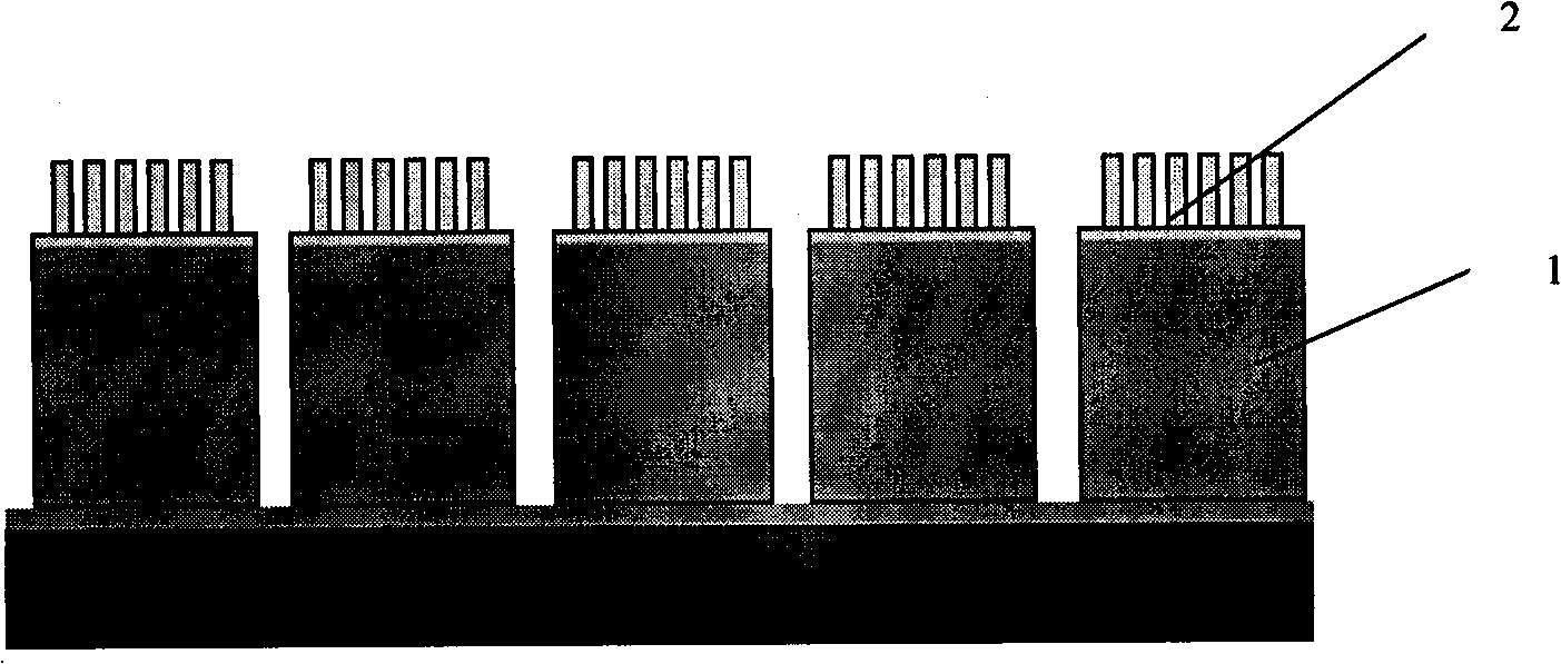
Nano ZnO semiconductor junction array and preparation method thereof
A nano-pillar array, semiconductor technology, applied in low-dimensional nano-materials and nano fields, can solve the problems of unreported semiconductor junctions, doping, etc., and achieve the effects of low cost, good lattice matching, and improved performance
- Summary
- Abstract
- Description
- Claims
- Application Information
AI Technical Summary
Problems solved by technology
Method used
Image

Examples
Embodiment 1
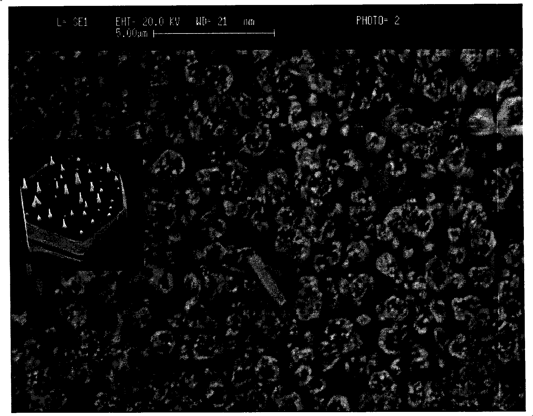
[0027] 1) First, the ZnO seed layer is prepared by CVD method: uniformly mix 600mg Zn powder and 60mg C powder (mixed source), put it into an alumina boat, and place the cleaned and dried Si sheet directly above it, and the Si sheet and The vertical distance of the mixing source is 4mm. Push the alumina boat equipped with the mixed source into the horizontal tube furnace, raise the tube furnace to 760 °C at a speed of 15 °C / min, keep it for 10 min, and take out the Si sheet after the furnace temperature drops to room temperature. At this time, a seed layer required by the solution method has been deposited on the downward side of the Si sheet.
[0028] 2) Then adopt solution method to grow array or quasi-array ZnO micro-nano columns on the ZnO seed layer prepared by CVD. An equal volume of 50mM zinc nitrate [Zn(NO 3 ) 2 ·6H 2 O] and 50mM hexamethylenetetramine [C 6 h 12 N 4 ] into 80ml solution. The prepared solution was heated to 95° C. on an electromagnetically stirr...
Embodiment 2
[0032] 1) First, the ZnO seed layer is prepared by CVD method: uniformly mix 600mg of Zn powder and 50mg of C powder (mixed source), put it into an alumina boat, and place the cleaned and dried Si sheet directly above it, and the Si sheet and The vertical distance of the mixing source is 4mm. Push the alumina boat equipped with the mixed source into the horizontal tube furnace, raise the tube furnace to 750 °C at a speed of 15 °C / min, keep it warm for 5 min, and take out the Si sheet after the furnace temperature drops to room temperature. At this time, a seed layer required by the solution method has been deposited on the downward side of the Si sheet.
[0033] 2) Then adopt solution method to grow array or quasi-array ZnO micro-nano columns on the ZnO seed layer prepared by CVD. An equal volume of 50mM zinc nitrate [Zn(NO 3 ) 2 ·6H 2 O] and 50mM hexamethylenetetramine [C 6 h 12 N 4 ] into 80ml solution. Add 0.2 mmol of In to the solution 2 o 3powder. The prepared ...
PUM
 Abstract
Description
Claims
Application Information