Lamb wave immune sensor and its device manufacturing method
An immune sensor and sensor technology, which is applied in the direction of instruments, scientific instruments, measuring devices, etc., can solve the problems of sensor arraying, high-throughput and large-sample molecular level measurement, etc., to achieve multi-channel detection and avoid missed detection , suitable for mass production
- Summary
- Abstract
- Description
- Claims
- Application Information
AI Technical Summary
Problems solved by technology
Method used
Image
Examples
Embodiment 1
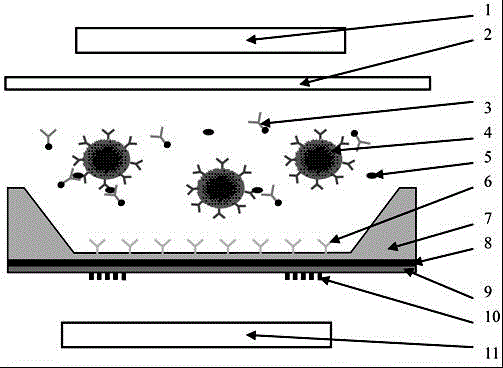
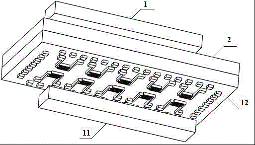
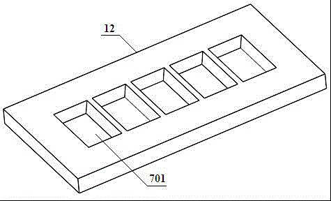
[0047] see figure 1 , figure 2 As shown, a Lamb wave immune sensor comprises an upper magnet 1 and a lower magnet 11, a Lamb wave sensor 12 is arranged between the upper magnet 1 and the lower magnet 11, and a pipeline pressure is glued above the Lamb wave sensor 12. cover 2; further, combine image 3 As shown, the Lamb wave sensor 12 includes a silicon thin film structure 7 provided with a plurality of sample cells 701, a conductive ground layer 8 below the silicon thin film structure 7, and a piezoelectric material layer 9 below the conductive ground layer 8 , the piezoelectric material layer 9 is provided with a layer of IDT electrode layer, further, combined Figure 4 As shown, the IDT electrode layer includes several interdigital electrodes 10 and several solder joint ports 13, a pair of electrode ports 14 are respectively arranged on the several interdigital electrodes 10, and labeled antibodies 3, Immunization of micromagnetic beads 4 and capture antibody 6; further...
Embodiment 2
[0054] see figure 1 Shown, a kind of manufacturing method of Lamb wave device, it comprises the following steps:
[0055] Step 1) Prepare silicon wafer: take a P-type (100) silicon wafer with 3 inches, 380 μm thick, double-sided oxidation, and surface thickness variation less than 3 μm;
[0056] Step 2) Photoresist removal: the silicon wafer is first cleaned with a mixture of acetone and alcohol, then soaked in deionized water for 5 minutes, then dried, and then the adhesive and photoresist are removed from both sides of the silicon wafer;
[0057] Step 3) Photolithography and development: use a photolithography machine to expose the silicon wafer, generate a pattern of the template on the surface of the silicon wafer, and then put it into the developer solution to etch to generate the required pattern on the photoresist layer;
[0058] Step 4) Etching silicon dioxide: put the silicon wafer into the hydrofluoric acid solution, etch the silicon dioxide layer, so that the patte...
Embodiment 3
[0071] see figure 1 Shown, a method for detecting carcinoembryonic antigen, it may further comprise the steps:
[0072] Step 1) Mix the analyte 5 with the immune micro-magnetic beads 4, inject them into the sample pool 701 of the Lamb wave device 12 and incubate together, and the surface of the immune micro-magnetic beads 4 is coated with a certain carcinoembryonic antigen antibody;
[0073] Step 2) Turn on the magnetic field under the Lamb wave immune sensor, so that the immune magnetic balls are adsorbed to the surface of the Lamb wave device 12, and together with the capture antibody 6 on the surface of the Lamb wave device 12, form a ternary compound of "immune magnetic balls-analyte-antibody" thing;
[0074] Step 3) Turn on the magnetic field above the Lamb wave immunosensor, so that the immune micro-magnetic beads 4 that have not formed the ternary complex of "immunomagnetic ball-analyte-antibody" are adsorbed to the top of the Lamb wave device 12;
[0075] Step 4) Add...
PUM
| Property | Measurement | Unit |
|---|---|---|
| thickness | aaaaa | aaaaa |
| height | aaaaa | aaaaa |
| diameter | aaaaa | aaaaa |
Abstract
Description
Claims
Application Information


