Groove flat-grid MOSFET component and fabricating method thereof

A manufacturing method and planar gate technology, applied in semiconductor/solid-state device manufacturing, semiconductor devices, electrical components, etc., can solve problems such as threshold voltage difficulty, breakdown voltage drop, process cost increase, etc., to facilitate popularization and utilization, manufacturing method The effect of simplicity and low process cost

Inactive Publication Date: 2009-09-23
XIAN UNIV OF TECH
View PDF0 Cites 22 Cited by
  • Summary
  • Abstract
  • Description
  • Claims
  • Application Information

AI Technical Summary

Problems solved by technology

However, when the breakdown voltage of VDMOS (U BR ) rises, its on-resistance (R on ) then rises sharply at a rate of about 2.5 powers, that is, R on =U BR 2.4~2.6 , leading to a large conduction loss in the VDMOS structure
Therefore, the VDMOS structure has been limited to use in the low voltage (<200V) range
In the existing trench gate MOSFET (VUMOS) structure, although the introduction of the trench can effectively reduce the on-resistance, the breakdown voltage is greatly reduced; and, since the channel of the VUMOS structure enters the body, the threshold Voltage a

Method used


Image

  • Groove flat-grid MOSFET component and fabricating method thereof
  • Groove flat-grid MOSFET component and fabricating method thereof
  • Groove flat-grid MOSFET component and fabricating method thereof

Examples


Embodiment Construction

[0032] The present invention will be described in detail below in conjunction with the accompanying drawings and specific embodiments.

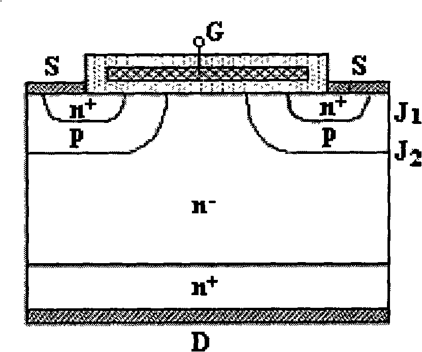
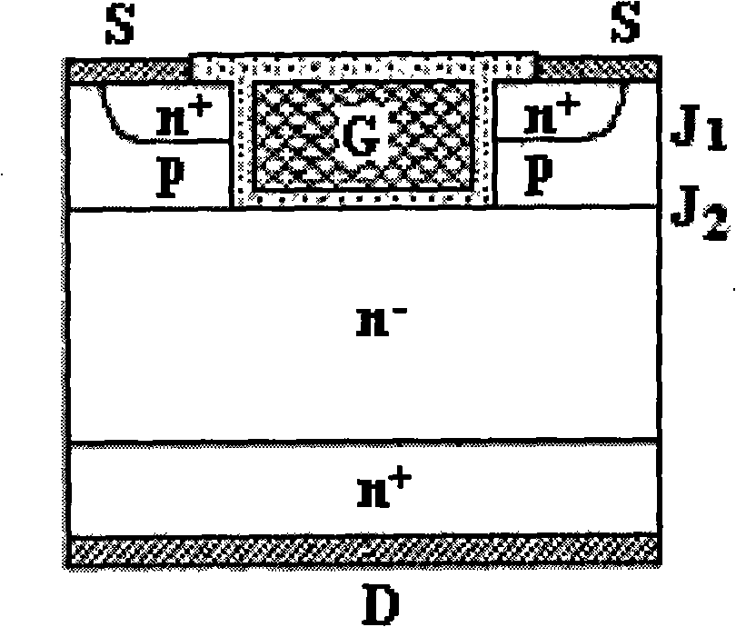
[0033] figure 1 and figure 2 They are schematic cross-sectional schematic diagrams of the basic structure of the existing planar gate VDMOS and trench gate VUMOS respectively. Depend on figure 1 It can be seen that the existing VDMOS structure is a planar gate, the channel is on the surface, and its length is composed of the p base region and the n + The difference between the lateral junction depths of the two diffusions in the source region is determined. Depend on figure 2 It can be seen that the trench gate of the existing trench gate VUMOS structure is connected to the source region, and the bottom of the trench enters the n - drift region, the channel is in the body, and its length is also determined by the p base region and n + The difference between the lateral junction depths of the two diffusions in the source region is dete...


PUM


Abstract

The invention discloses a groove flat-grid MOSFET component which comprises an n<-> epitaxial layer connected to the upside of an n<+> silicon substrate layer, wherein a flat-grid G is arranged above the n<-> epitaxial layer, the epitaxial layers at two sides of the flat-grid G are respectively provided with a p base region which is internally provided with an n<+> source region, and a source electrode is formed by short circuit between the n<+> source region and the p base region. The groove flat-grid MOSFET component is characterized in that a groove is arranged between the two p base regions along the middle of the upper end of the n<-> epitaxial layer, the inner part of the groove is filled with a polysilicon gate, gate oxide is filled between the polysilicon gate and the n<-> epitaxial layer, and the gate oxide and the polysilicon gate are respectively connected with gate oxide and polysilicon gate of the flat part above the n<-> epitaxial layer into a whole. The groove flat-grid MOSFET component improves the electric breakdown strength of the component, reduces the on resistance, keeps switch loss unchangeable, increases design and fabrication freedom, has low fabrication cost, and is completely compatible with the prior VDMOS process.

Description

technical field [0001] The invention belongs to the technical field of power semiconductor devices, and relates to a trench planar gate MOSFET device, and also relates to a manufacturing method of the trench planar gate MOSFET device. Background technique [0002] Breakdown voltage and on-resistance are two main parameters that must be considered in designing power MOSFET devices. If the breakdown voltage is increased, the on-resistance will also increase, resulting in an increase in on-state power consumption. Since there is an irreconcilable contradiction between the on-resistance and the breakdown voltage, in practical applications, it is necessary to limit the on-resistance of the power MOSFET device. [0003] The existing planar gate power MOSFET (VDMOS) structure has a simple manufacturing process, so it has been widely used in high-frequency and low-power applications. However, when the breakdown voltage of VDMOS (U BR ) rises, its on-resistance (R on ) then rises...

Claims


Application Information

Patent Timeline
IPC IPC(8): H01L29/78H01L29/06H01L29/423H01L21/336
CPCH01L29/42376H01L29/7813
Inventor 王彩琳孙丞
Owner XIAN UNIV OF TECH
Why Eureka
Try Eureka