GeTe/Sb2Te3 multilayer nanocomposite phase transition film and preparation method
A nano-composite and thin-film technology, applied in the field of materials in the field of microelectronics technology, can solve problems such as large RESET current, low crystalline resistivity, and affecting the storage speed of phase-change memory, and achieve the effect of ensuring reliability
- Summary
- Abstract
- Description
- Claims
- Application Information
AI Technical Summary
Problems solved by technology
Method used
Image
Examples
Embodiment 1
[0024] Step 1 Clean SiO 2 / Si(100) substrate surface and back, remove dust particles, organic and inorganic impurities:
[0025] a) Strong ultrasonic cleaning in acetone solution for 3-5 minutes, then rinse with deionized water;
[0026] b) Strong ultrasonic cleaning in ethanol solution for 3-5 minutes, rinse with deionized water, high-purity N 2 Blow dry the watch and back;
[0027] c) Dry the water vapor in an oven at 120°C for about 20 minutes.
[0028] Step 2 Prepare GeTe and Sb by room temperature magnetron sputtering 2 Te 3 Phase change film preparation:
[0029] a) Prepare GeTe and Sb with a diameter of 50.8mm and a thickness of 5mm 2 Te 3 Alloy target, the purity of the alloy target is 99.999% (atomic percentage), the background vacuum reaches 1×10 -4 Pa;
[0030] b) The radio frequency power is set at 20W;
[0031] c) Ar gas with a purity of 99.999% is used as the sputtering gas, the gas flow rate is controlled at 30 SCCM, and the sputtering pressure is 0.2 ...
Embodiment 2
[0037] Step 1, step 2 are identical with embodiment 1;
[0038] Step 3: Prepare GeTe / Sb by room temperature magnetron alternate sputtering method 2 Te 3 Nanocomposite multilayer phase change film:
[0039] a) Rotate the substrate to Sb 2 Te 3 target, open Sb 2 Te 3 RF power on the target, start sputtering Sb 2 Te 3 thin film, the sputtering time is 2s;
[0040] b) Sb 2 Te 3 After film sputtering is complete, turn off the Sb 2 Te 3 The RF power applied on the target, the substrate is rotated to the GeTe target position, the RF power on the GeTe target is turned on, and the GeTe thin film is sputtered, and the sputtering time is 6s;
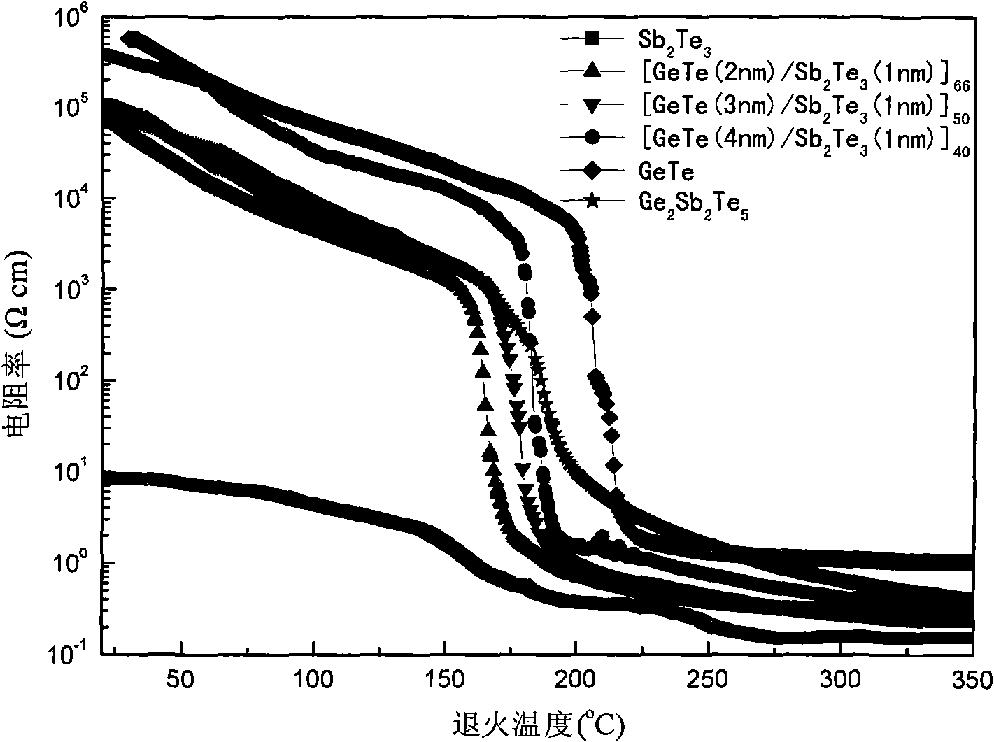
[0041] c) Repeat a) and b) two steps, that is, in SiO 2 / Si(100) substrate prepared film structure as [GeTe(3nm) / Sb2Te3(1nm)] 50 The nanocomposite multilayer phase change film, the total thickness of the film is controlled at 200nm.
Embodiment 3
[0043] Step 1, step 2 are identical with embodiment 1;
[0044] Step 3: Prepare GeTe / Sb by room temperature magnetron alternate sputtering method 2 Te 3 Nanocomposite multilayer phase change film:
[0045] a) Rotate the substrate to Sb 2 Te 3 target, open Sb 2 Te 3 RF power on the target, start sputtering Sb 2 Te 3 thin film, the sputtering time is 2s;
[0046] b) Sb 2 Te 3 After film sputtering is complete, turn off the Sb 2 Te 3 The RF power applied on the target, the substrate is rotated to the GeTe target position, the RF power on the GeTe target is turned on, and the GeTe thin film is sputtered, and the sputtering time is 8s;
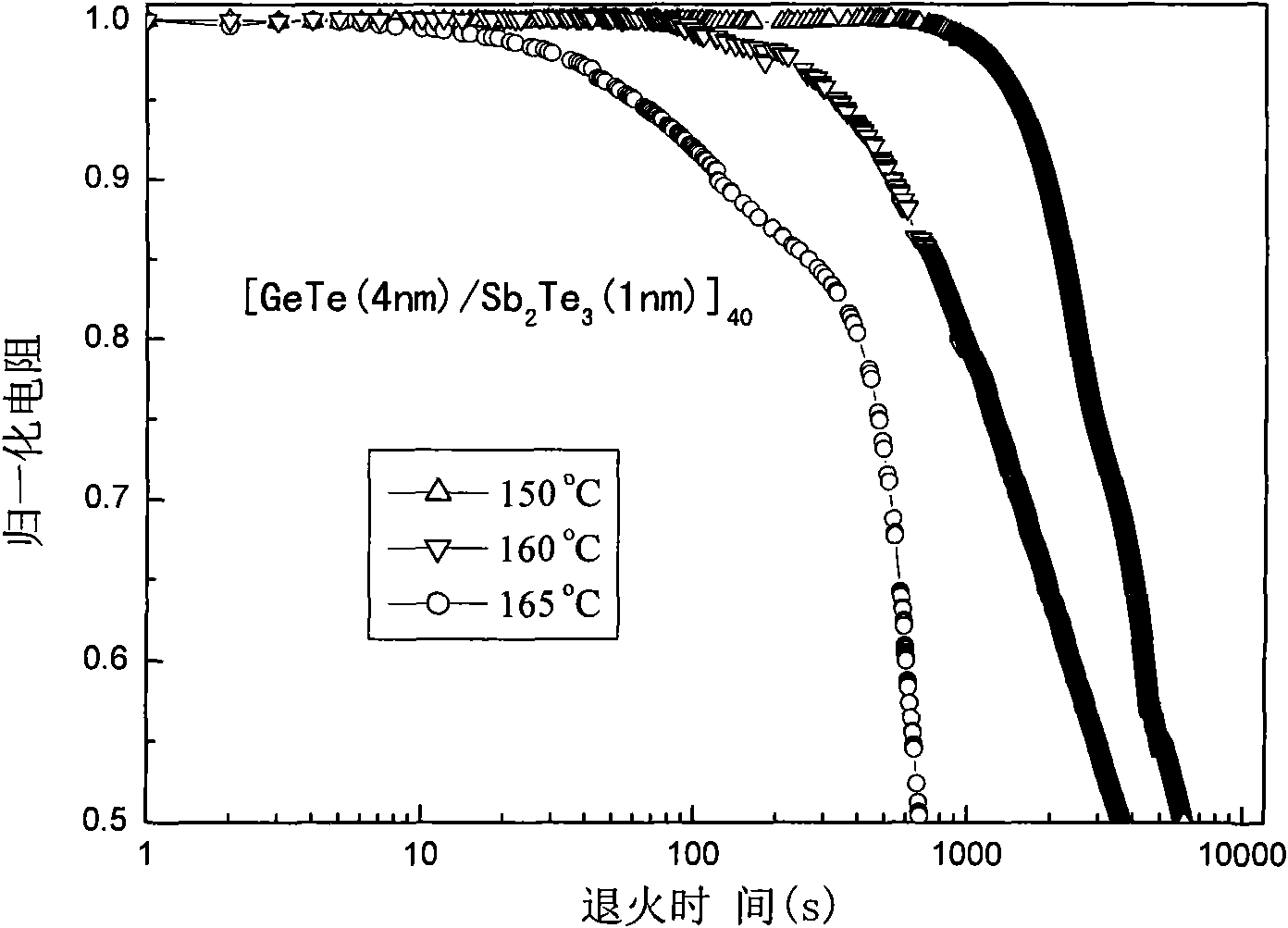
[0047] c) Repeat a) and b) two steps, that is, in SiO 2 / Si(100) substrate prepared film structure as [GeTe(4nm) / Sb2Te3(1nm)] 40 The nanocomposite multilayer phase change film, the total thickness of the film is controlled at 200nm.
PUM
| Property | Measurement | Unit |
|---|---|---|
| thickness | aaaaa | aaaaa |
| thickness | aaaaa | aaaaa |
| crystallization temperature | aaaaa | aaaaa |
Abstract
Description
Claims
Application Information


