Method for synthesizing tellurium-contained semiconductor nanocrystal
A synthesis method and semiconductor technology, applied in the fields of selenium/tellurium compounds, chemical instruments and methods, inorganic chemistry, etc., can solve the problems of toxic, flammable and explosive, and reduce the cost of synthesizing nanocrystals, and achieve easy operation, cost saving, and improvement of The effect of synthesis efficiency
- Summary
- Abstract
- Description
- Claims
- Application Information
AI Technical Summary
Problems solved by technology
Method used
Image

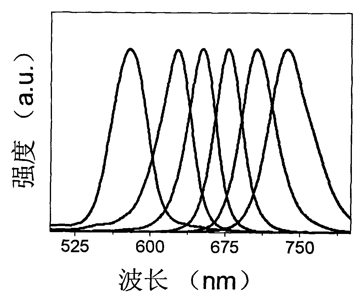
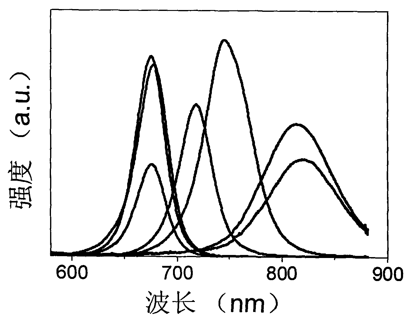
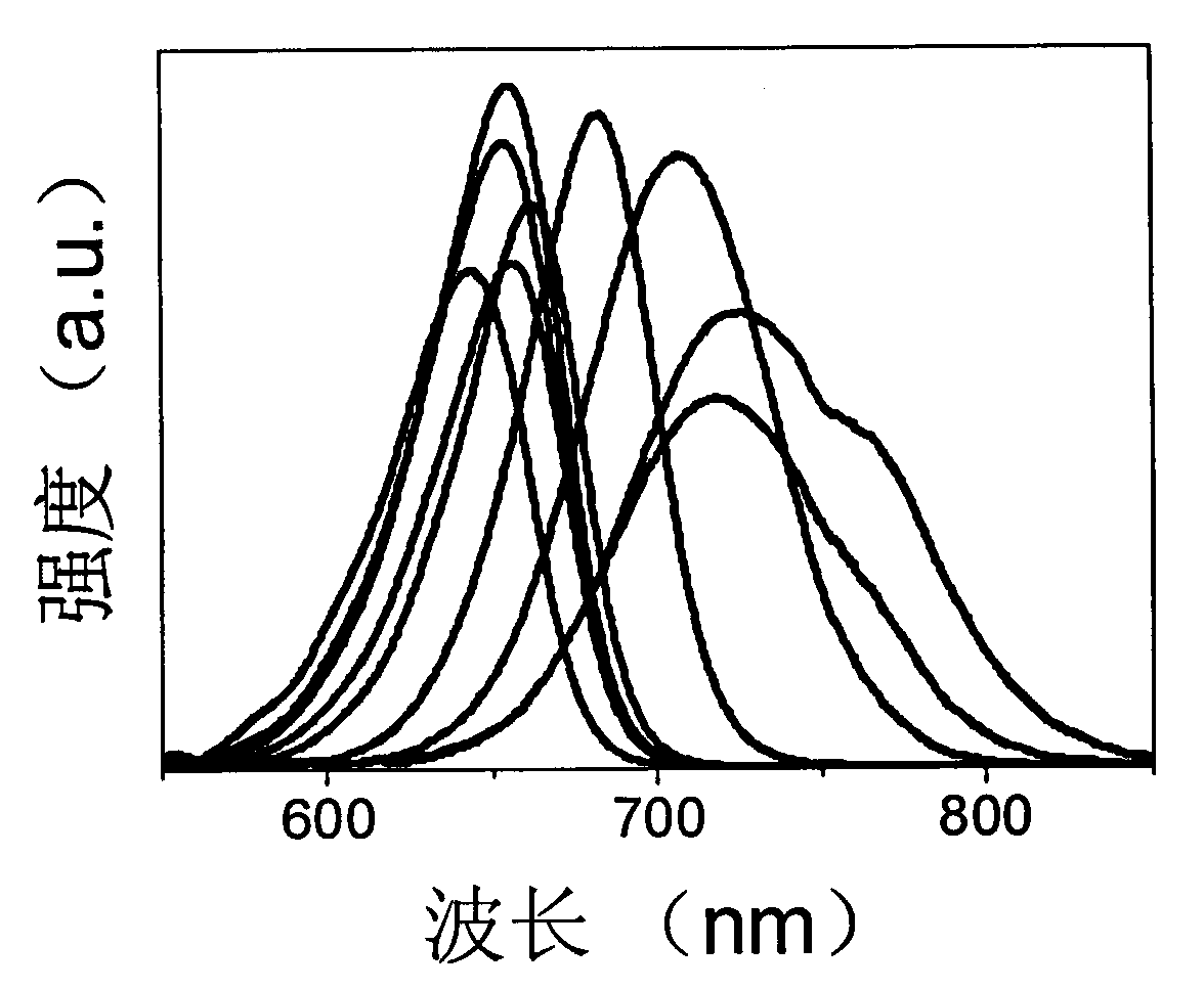
Examples
Embodiment 1-2
[0024] The preparation of embodiment 1-2CdTe nanocrystal
Embodiment 1
[0026] Add 1mmol Te powder to 10g trioctylphosphine oxide TOPO and heat to 380°C under nitrogen atmosphere until Te is completely dissolved to obtain a light yellow solution that is the Te precursor, which is cooled for later use.
[0027] 0.1 mmol of cadmium decacarbonate and 4 g of octadecene were mixed into a 25 mL three-neck flask, and heated to 240° C. (180-350° C. is acceptable) under nitrogen atmosphere to obtain a clear and uniform solution, namely the cadmium precursor.
[0028] Take 1g of Te precursor solution and inject it into the Cd solution at 240°C, and take samples for observation at different times. After reacting for 3 hours, cool down, add methanol to precipitate, and centrifuge to obtain CdTe nanocrystals.
Embodiment 2
[0030] Add 1mmol Te powder to 10g trioctylphosphine oxide TOPO and heat to 380°C under nitrogen atmosphere until Te is completely dissolved to obtain a light yellow solution that is the Te precursor, which is cooled for later use.
[0031] 0.4 mmol of cadmium decacarbonate and 6 g of octadecene were mixed into a 25 mL three-necked flask, and heated to 320° C. (180-350° C. was acceptable) under nitrogen atmosphere to obtain a clear and homogeneous solution, namely the cadmium precursor.
[0032] Take 2g of Te precursor solution and inject it into the Cd solution at 300°C, and take samples for observation at different times. After reacting for 3 hours, cool down, add methanol to precipitate, and centrifuge to obtain CdTe nanocrystals.
PUM
 Abstract
Description
Claims
Application Information
 - R&D
- Intellectual Property
- Life Sciences
- Materials
- Tech Scout
- Unparalleled Data Quality
- Higher Quality Content
- 60% Fewer Hallucinations
Browse by: Latest US Patents, China's latest patents, Technical Efficacy Thesaurus, Application Domain, Technology Topic, Popular Technical Reports.
© 2025 PatSnap. All rights reserved.Legal|Privacy policy|Modern Slavery Act Transparency Statement|Sitemap|About US| Contact US: help@patsnap.com