Optical disc manufacturing method, disc master manufacturing method, and optical disc
A manufacturing method and optical disc technology, applied in the direction of optical record carrier manufacturing, optical record carrier, etc., can solve the problem of increasing resolution, etc.
- Summary
- Abstract
- Description
- Claims
- Application Information
AI Technical Summary
Problems solved by technology
Method used
Image
Examples
Embodiment Construction
[0063] Embodiments of the present invention will be described according to the following order:
[0064] [1. Disc manufacturing process],
[0065] [2. Mastering using inorganic resist],
[0066] [3. The disc to be manufactured], and
[0067] [4. Verification]
[0068] [1. Disc manufacturing process]
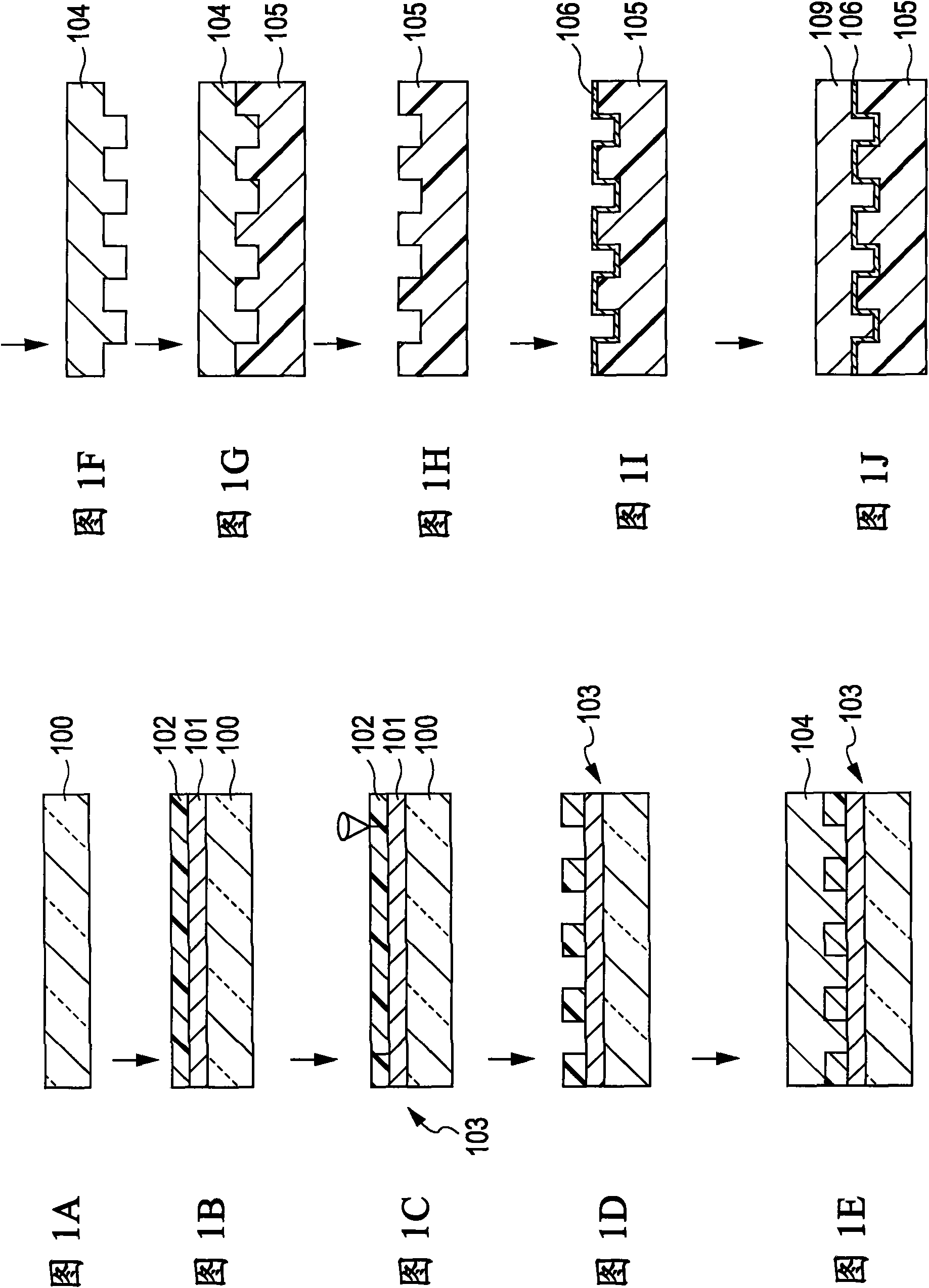
[0069] First refer to Figure 1A ~ Figure 1J A schematic diagram is shown to describe the process used to manufacture an optical disc.
[0070] Figure 1A A master forming substrate 100 providing a disc master is shown. For example, the mastering substrate 100 may be made of a silicon wafer or quartz.
[0071] Such as Figure 1B As shown, a heat storage layer 101 and an inorganic resist layer 102 are deposited on a master forming substrate 100 by sputtering.
[0072] Next, if Figure 1C As shown, the resulting resist layer is photosensitive by performing selective exposure corresponding to the pit array (used as a recording signal pattern) on the inorganic resist layer ...
PUM
| Property | Measurement | Unit |
|---|---|---|
| depth | aaaaa | aaaaa |
| depth | aaaaa | aaaaa |
| wavelength | aaaaa | aaaaa |
Abstract
Description
Claims
Application Information


