
Method for preparing carbon nanofiber
A technology of carbon nanofibers and direct current electric field, applied in nanotechnology, nanotechnology, nanostructure manufacturing, etc., can solve problems such as limited applicability and effectiveness, difficulty in accurately controlling the diameter of CNFs, and enlarged diameter distribution range , to achieve the effect of uniform size, strong applicability, and simple electric field device
- Summary
- Abstract
- Description
- Claims
- Application Information
AI Technical Summary
Problems solved by technology
Method used
Image

Examples
Embodiment 1
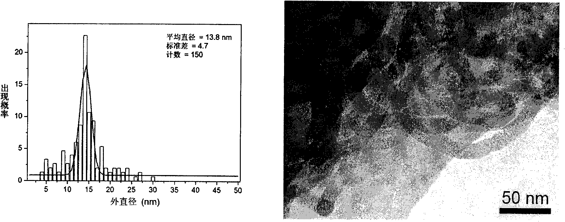
[0026] Example 1: After the deposited substrate numbered M2 was placed in the CVD uniform temperature zone, the furnace chamber was closed, and Ar gas was introduced at a flow rate of 200 sccm, and heated to 600° C. after 40 minutes. At this time, an external electric field is introduced, and the substrate is connected to the negative electrode of the electric field, and the electric field intensity is kept constant at 25000V / m. Inject C at a flow rate of 30 sccm 2 h 2 Gas, the reaction starts and lasts for 3 minutes; after the reaction is completed, turn off the C 2 h 2 Remove the external electric field from the gas valve, and take it out after cooling to room temperature under the protection of Ar gas. The obtained carbon nanofiber transmission electron microscope (TEM) picture and diameter distribution figure are shown in figure 2 ,Such as figure 2 As shown, the average diameter is 13.8nm, and the standard error is 4.7nm.
Embodiment 2
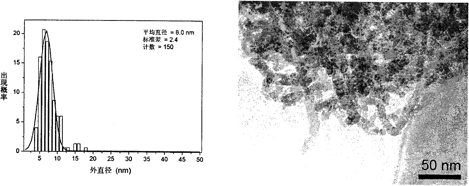
[0027] Example 2: Apply an electric field of 50000 V / m to the deposited substrate numbered M3 (other experimental conditions are the same as in Example 1). The obtained carbon nanofiber transmission electron microscope (TEM) picture and diameter distribution figure are shown in image 3 ,Such as image 3 As shown, the average diameter is 8.0 nm, and the standard error is 2.4 nm.
Embodiment 3
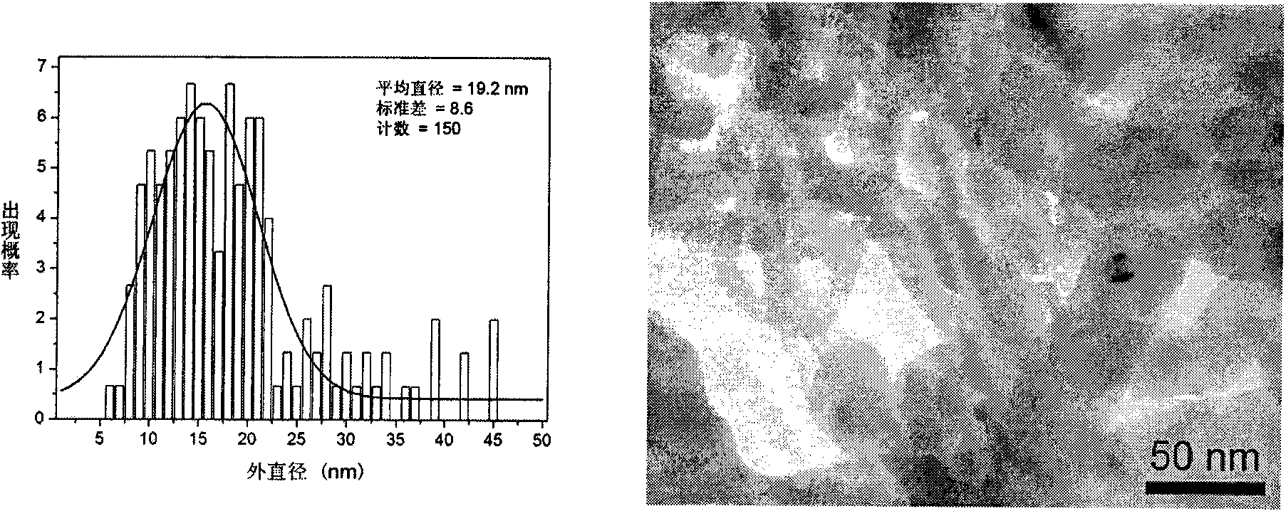
[0028] Example 3: As a comparison, the deposited substrate numbered M1 was also put into CVD, and the experimental conditions were the same as in Example 1, but no electric field was added during the preparation process. The obtained carbon nanofiber transmission electron microscope (TEM) picture and diameter distribution figure are shown in figure 1 ,Such as figure 1 As shown, the average diameter is 19.2 nm, and the standard error is 8.6 nm.
[0029] It can be seen from the above that with the increase of the applied electric field, the average diameter of CNFs and the diameter distribution range are gradually reduced, that is, the purpose of controlling the diameter of CNFs is achieved.
PUM
| Property | Measurement | Unit |
|---|---|---|
| diameter | aaaaa | aaaaa |
| diameter | aaaaa | aaaaa |
| diameter | aaaaa | aaaaa |
Abstract
Description
Claims
Application Information