Method for improving thickness consistency of oxide layer on side wall of grid electrode and method for manufacturing grid electrode

A technology of oxide layer thickness and gate sidewall, which is applied in the manufacture of gates and semiconductor devices, can solve problems such as process complexity, etching process slowdown, and gate line width changes

Inactive Publication Date: 2009-11-04
SEMICONDUCTOR MANUFACTURING INTERNATIONAL (BEIJING) CORP
View PDF1 Cites 13 Cited by
  • Summary
  • Abstract
  • Description
  • Claims
  • Application Information

AI Technical Summary

Problems solved by technology

[0015] Although the method of the above-mentioned U.S. patent can improve the thickness uniformity of the oxide layer on the sidewall of the formed gate to a certain extent, this method requires multi-step etching and plasma oxidation treatment processes, so that the etching process is slowed down, and the process Complicated; moreover, the oxidation process in the etching process may cause the line width of the gate to change

Method used


Image

  • Method for improving thickness consistency of oxide layer on side wall of grid electrode and method for manufacturing grid electrode
  • Method for improving thickness consistency of oxide layer on side wall of grid electrode and method for manufacturing grid electrode
  • Method for improving thickness consistency of oxide layer on side wall of grid electrode and method for manufacturing grid electrode

Examples


Embodiment 1

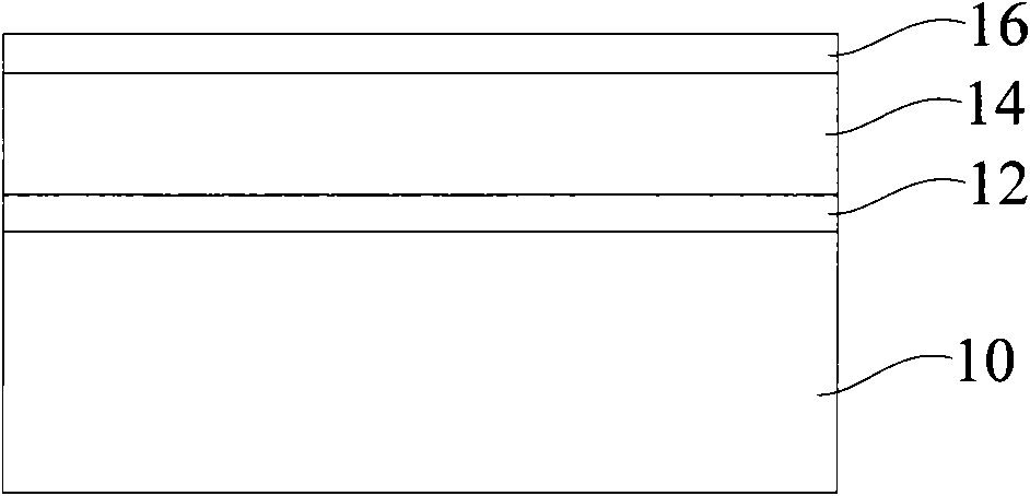
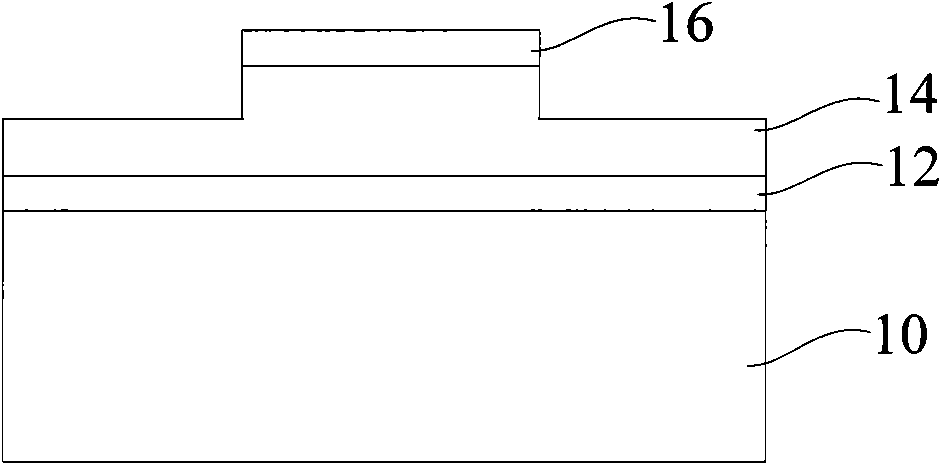
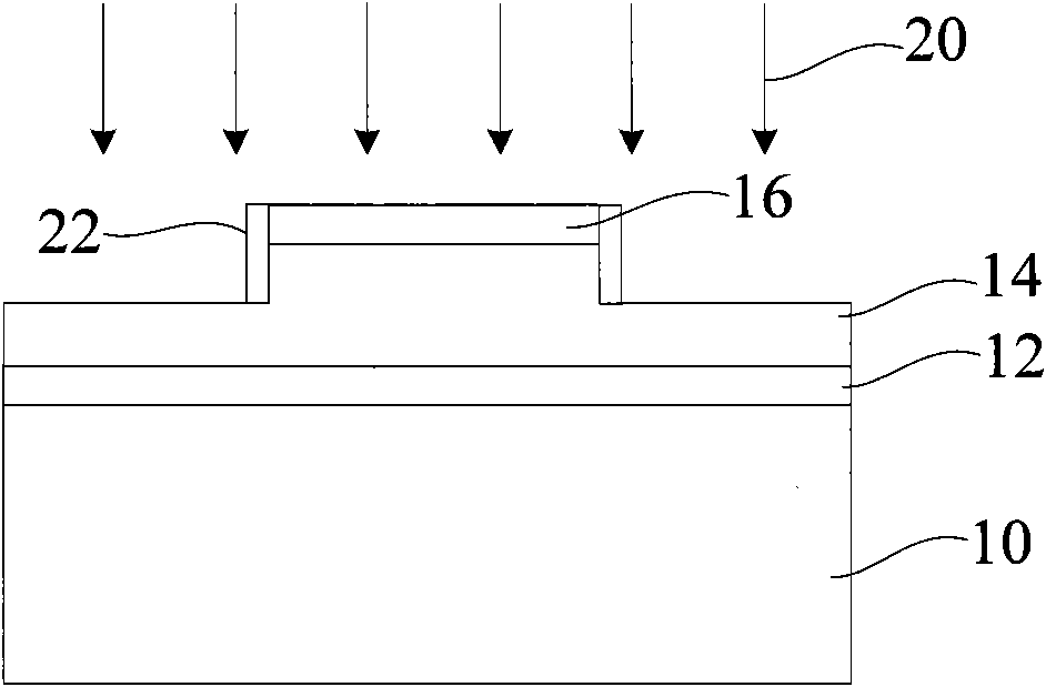
[0052] Please refer to Figure 5 Firstly, a semiconductor substrate 100 is raised, on which there is a gate dielectric layer 102 and a polysilicon layer 104 as a gate, and the polysilicon layer 104 is located on the gate dielectric layer 102 .

[0053] Wherein, the gate can also be a stacked structure of a polysilicon layer and other structures, such as Figure 7 The gate shown is a stacked structure of a polysilicon layer 104 and a metal silicide layer 105, and the metal silicide layer 105 is located on the polysilicon layer 104 to reduce the resistivity of the formed gate and improve the performance of the device;

[0054] another example Figure 8The gate shown is a stacked structure of a first polysilicon layer 104, a dielectric layer 105 and a second polysilicon layer 107, and the dielectric layer 105 is located between the first polysilicon layer 104 and the second polysilicon layer 107 Between; the dielectric layer 105 may be a stacked structure of silicon oxide-silic...

Embodiment 2

[0071] Embodiment 2 is still based on Figure 5 and Figure 6 Reference for explanation.

[0072] In this embodiment, before the in-situ water vapor generation oxidation is performed, an annealing process may be performed on the gate electrode containing the doped polysilicon layer, so that the impurity ions in the polysilicon layer are redistributed, thereby improving the performance of the polysilicon layer. The uniformity of the distribution of impurity ions reduces the influence of the uneven distribution of the ions on the thickness of the formed gate sidewall oxide layer, and then performs the in-situ water vapor oxidation process to further increase the thickness of the gate sidewall oxide layer Uniformity.

[0073] Detailed description will be given below.

[0074] Please refer to Figure 5 , firstly, a semiconductor substrate 100 is raised, on which there is a gate dielectric layer 102 and a polysilicon layer 104 as a gate, and the polysilicon layer 104 is located...


PUM


Abstract

The invention relates to a method for improving the thickness consistency of an oxide layer on the side wall of a grid electrode, and provides a semiconductor substrate, wherein the grid electrode comprising a polysilicon layer is arranged on the semiconductor substrate, and foreign ions are doped in the polysilicon layer; and the grid electrode is subjected to in-situ water vapor generation oxidation process, and the oxide layer is formed on the side wall of the grid electrode, wherein the temperature in the in-situ water vapor generation oxidation process is between 800 and 1,500 DEG C. The invention also provides a method for manufacturing the grid electrode. The method can improve the thickness consistency of the oxide layer on the side wall of the grid electrode and has simple process.

Description

technical field [0001] The invention relates to the technical field of semiconductor manufacturing, in particular to a method for manufacturing a gate and a method for manufacturing a semiconductor device. Background technique [0002] A metal oxide semiconductor device includes a gate, a source, and a drain. Wherein, the gate is mostly made of polysilicon material. An existing step for forming a polysilicon gate is as follows: [0003] forming a gate dielectric layer on the semiconductor substrate, and depositing a polysilicon layer on the gate dielectric layer; [0004] spin-coating a photoresist layer on the polysilicon layer, and patterning the photoresist layer to form a gate pattern; [0005] Etching and removing the polysilicon layer not covered by the gate pattern, transferring the photoresist pattern into the polysilicon layer to form a gate; [0006] Since the anisotropic dry etching is used in the etching, the plasma of the dry etching will destroy the lattice...

Claims


Application Information

Patent Timeline
Patent Type & Authority Applications(China)
IPC IPC(8): H01L21/28H01L21/316H01L21/336
Inventor 魏莹璐居建华
Owner SEMICONDUCTOR MANUFACTURING INTERNATIONAL (BEIJING) CORP
Why Eureka
Try Eureka