Packaging housing of humidity-sensitive electronic device, substrate and leakproof structure thereof
A technology for encapsulating shells and electronic devices, applied in the direction of electric solid devices, piezoelectric/electrostrictive/magnetostrictive devices, electrical components, etc., can solve the problem of reducing the bonding performance of the substrate and the encapsulating shell, and achieve good adhesion Performance and encapsulation effect, effect of encapsulation effect improvement
- Summary
- Abstract
- Description
- Claims
- Application Information
AI Technical Summary
Problems solved by technology
Method used
Image
Examples
Embodiment 1
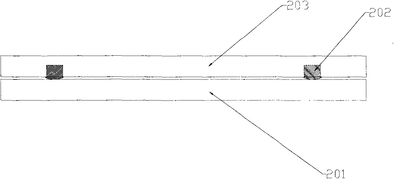
[0020] Glass substrate / ITO / NPB(50nm) / Alq(50nm) / Mg:Ag / glass sheet with a ring of grooves
[0021] (1) Cleaning of glass substrates pre-engraved with ITO: use hot detergent ultrasonic and deionized water ultrasonic methods to clean the transparent conductive substrate ITO glass, place it under an infrared lamp to dry after cleaning, and then The dried ITO glass is pretreated by ultraviolet ozone cleaning and low-energy oxygen ion beam bombardment. The ITO film on the conductive substrate is used as the anode layer of the device. The square resistance of the ITO film is 50Ω and the film thickness is 150nm;
[0022] (2) Preparation of the organic light-emitting layer: the above-mentioned cleaned and dried ITO glass that has been pretreated is placed in a vacuum chamber, and the vacuum is evacuated to 1×10 -3 Pa, and then evaporate a layer of hole transport material NPB on the above-mentioned ITO film, the evaporation rate of the material film is 0.5nm / s, and the film thickness is ...
Embodiment 2
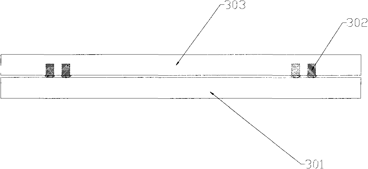
[0026] Glass substrate / ITO / NPB / Alq / Mg:Ag / PI / glass sheet with two grooves
[0027] The preparation steps are the same as in Example 1, except that two circles of grooves 302 with a depth of 1 mm and a width of 0.75 mm are made on the packaging glass 303, glue is dispensed on the two circles of grooves, and then the packaging glass 303 is pressed together and the substrate 301, the thickness of the sealing material exposed to gas was 4 μm.
PUM
| Property | Measurement | Unit |
|---|---|---|
| Sheet resistance | aaaaa | aaaaa |
| Film thickness | aaaaa | aaaaa |
| Film thickness | aaaaa | aaaaa |
Abstract
Description
Claims
Application Information


