Irradiation resistant multi-interdigital CMOS device

A multi-finger, anti-radiation technology, applied in the field of electronics, can solve problems such as large gate parasitic resistance, troublesome circuit design, and large layout area, and achieve the effect of reducing gate series resistance, reducing layout area, and improving integration.

Inactive Publication Date: 2011-11-09
SEMICON MFG INT (BEIJING) CORP +1
View PDF0 Cites 0 Cited by
  • Summary
  • Abstract
  • Description
  • Claims
  • Application Information

AI Technical Summary

Problems solved by technology

However, due to the large layout area occupied by the ring structure, the large parasitic resistance of the gate, the inability to manufacture devices with small trench width / ditch length ratios, and the fact that each aspect ratio device must be designed separately, it brings great trouble to the circuit design. , so the application is limited

Method used


Image

  • Irradiation resistant multi-interdigital CMOS device
  • Irradiation resistant multi-interdigital CMOS device
  • Irradiation resistant multi-interdigital CMOS device

Examples


Embodiment Construction

[0037] The present invention will be further described below through specific embodiments in conjunction with the accompanying drawings.

[0038] In this embodiment, the multi-digit CMOS device of the present invention is prepared. The preparation method includes the following steps. The various methods mentioned are common methods well known to those of ordinary skill in the art, and the details will not be repeated here.

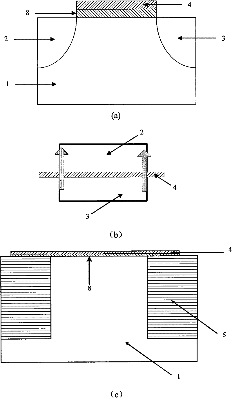
[0039] 1) Thermally grow silicon dioxide 9 and CVD (chemical vapor deposition) silicon nitride 11 on the P-type silicon substrate 1 as a mask, such as Figure 5 a;

[0040]2) Etching silicon dioxide 9 and silicon nitride 11 by photolithography technology, and etching silicon substrate 1 to form Figure 5 The groove shown in b;

[0041] 3) Deposit the STI oxide layer 5, and use chemical mechanical polishing technology to planarize the surface;

[0042] 4) Doping the channel by photolithography to form a P-type doped region 12, thermally growing a layer o...


PUM


Abstract

The invention discloses an irradiation resistant multi-interdigital CMOS device, belonging to the technical field of electron and comprising an active area, an STI area and a grid electrode, wherein the grid electrode is connected with the active area and the STI area and is in a multi-interdigital shape. The irradiation resistant multi-interdigital CMOS device is characterized in that the width of the active area along the transverse direction of the active area is longer than the width of the grid electrode along the transverse direction of the active area within the range of the active area; preferably, inner contour lines of root parts of two adjacent fingers are not in a fold line shape with each break angle of 90 degrees, and outer contour lines of root parts of two fingers positioned on the end part of the irradiation resistant multi-interdigital CMOS device are not in a right-angle shape. The irradiation resistant multi-interdigital CMOS device can effectively reduce the grid series resistance, thereby enhancing the performance of a circuit; and in addition, the invention also reduces the domain occupying area, thereby enhancing the integration level of a chip.

Description

technical field [0001] The invention relates to a semiconductor device, in particular to a novel anti-radiation multi-finger CMOS device, which belongs to the field of electronic technology. Background technique [0002] Integrated circuit chips have the advantages of small size, light weight, long life, high reliability, and good performance. At the same time, due to its low cost, it is easy to mass-produce and become the core of various electronic devices, and is widely used in various fields of production and life. An integrated circuit is a circuit module with specific functions composed of basic semiconductor devices. Devices applied to integrated circuits have experienced the evolution process from bipolar transistors to field effect transistors to complementary metal oxide field effect transistors (CMOS). CMOS devices are widely used in integrated circuit chips because of their low power consumption, high speed, and good integration. Now 95% of integrated circuits a...

Claims


Application Information

Patent Timeline
Patent Type & Authority Patents(China)
IPC IPC(8): H01L27/092H01L29/78H01L29/06H01L29/423
Inventor 王文华黄德涛黄如王阳元薛守斌
Owner SEMICON MFG INT (BEIJING) CORP
Why Eureka
Try Eureka