

Method for regulating wavelength of light emitted by LED through stress and corresponding white light LED
A luminous wavelength, white light technology, applied in the direction of semiconductor devices, electrical components, circuits, etc., can solve the problems of phosphor powder anti-ultraviolet degradation packaging materials that need to be further studied, ultraviolet LEDs are difficult to obtain, and low doping efficiency , to achieve high electrical conversion efficiency, simple circuit, and convenient preparation method
- Summary
- Abstract
- Description
- Claims
- Application Information
AI Technical Summary
Problems solved by technology
Method used
Image

Examples
Embodiment 1
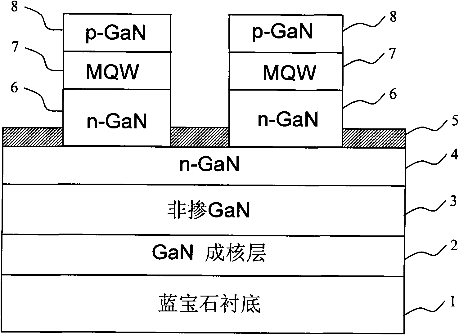
[0023] The structure of the GaN-based LED device of the present invention is as follows figure 1 As shown, on the sapphire substrate 1 are GaN nucleation layer 2, non-doped GaN layer 3, first n-type GaN layer 4 and SiO 2 A growth window is opened on the mask 5, and a second n-type GaN layer 6, a blue-light active layer 7 and a p-type GaN layer 8 are grown sequentially at the growth window. Through the stress adjustment of the growth window, the LED can emit purple light. The specific preparation process is as follows:
[0024] 1. With common metal organic chemical vapor deposition (MOCVD) equipment, substrate 1 adopts the sapphire substrate of (0001) face, hydrogen (H 2 ) atmosphere, bake the substrate at a high temperature of 1100°C to 1150°C for 5 to 15 minutes, cool down to 450°C to 550°C, and grow a GaN nucleation layer 2 with a thickness of 25nm at low temperature using trimethylgallium and ammonia as sources , and then increase the temperature to 1050°C to grow a 2000n...
Embodiment 2
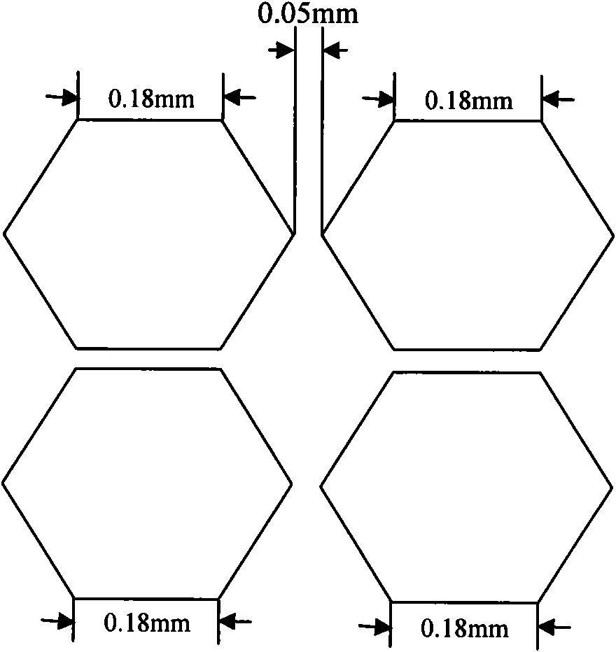
[0033] The preparation steps are the same as in Example 1, wherein the basic unit pattern of the growth window in step 4 is as follows image 3 As shown, the growth window is a regular hexagon with a side length of 180 μm, and the shortest distance between adjacent regular hexagons is 0.05 mm. The electroluminescence spectra of the obtained samples are shown in Figure 6 As shown in b) (measurement condition is the same as embodiment one), send yellow-green fluorescence
Embodiment 3
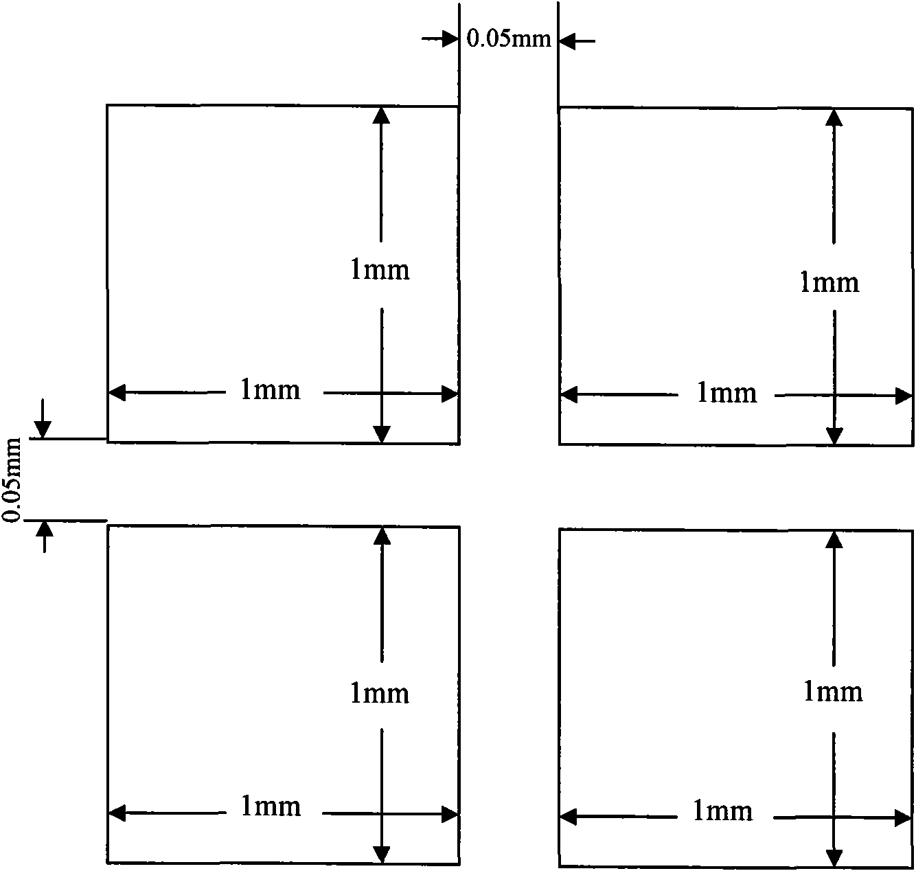
[0035] The preparation steps are the same as in Example 1, wherein the basic unit pattern of the growth window in step 4 is as follows Figure 4 As shown, the growth window is a circle with a diameter of 350 μm, and the shortest distance between adjacent circles is 0.05 mm. The electroluminescence spectra of the obtained samples are shown in Figure 6 As shown in c) (measurement condition is the same as embodiment one), send blue-purple fluorescence
PUM
 Abstract
Description
Claims
Application Information