
Method for forming gate of semiconductor device

A technology for semiconductors and devices, applied in the field of forming gates of semiconductor devices, can solve problems such as degraded surface roughness, reduced lifetime of gate oxide layers, and degraded device characteristics

Inactive Publication Date: 2009-12-16
KEY FOUNDRY CO LTD
View PDF3 Cites 12 Cited by
  • Summary
  • Abstract
  • Description
  • Claims
  • Application Information

AI Technical Summary

Problems solved by technology

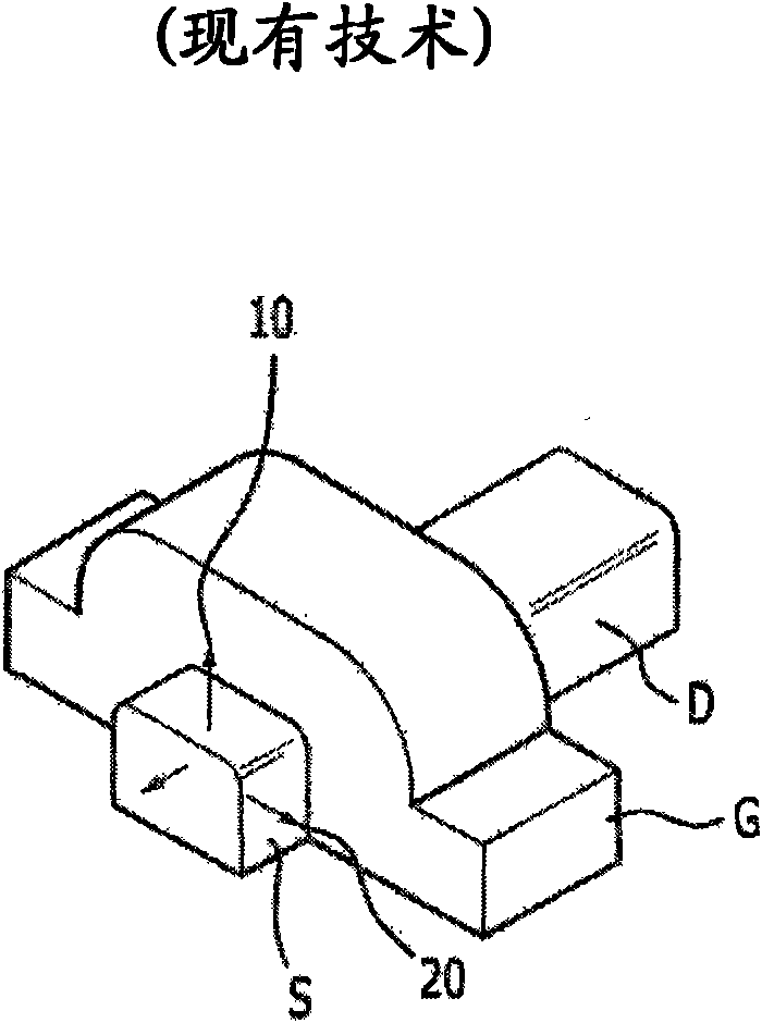
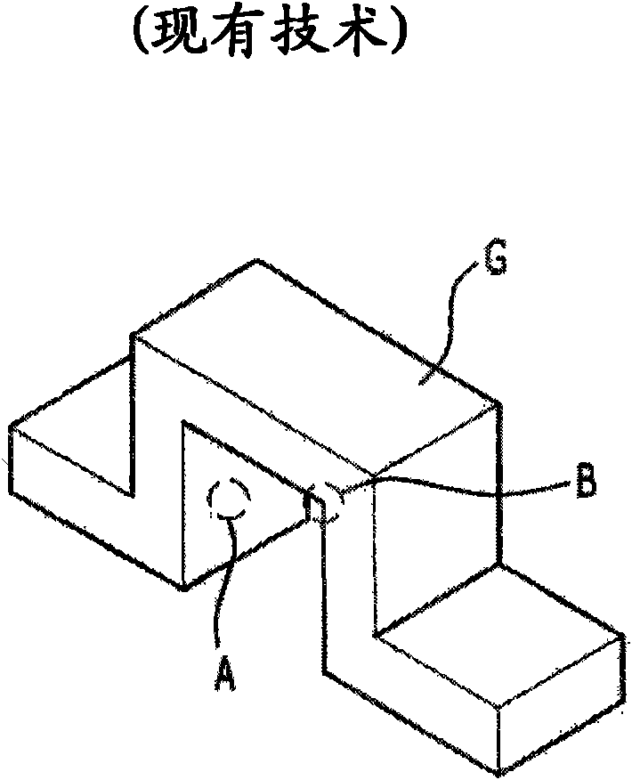
[0013] First, plasma damage leads to crystal defects
If crystal defects caused by plasma damage occur in side A serving as a channel, device characteristics deteriorate
In particular, the reliability of the device decreases
[0014] Second, the use of the plasma etching process deteriorates the surface roughness, such as striations that inevitably form in side A during the plasma etching process
Therefore, the failure of the gate oxide layer is caused, or the lifetime of the gate oxide layer is reduced

Method used


Image

  • Method for forming gate of semiconductor device
  • Method for forming gate of semiconductor device
  • Method for forming gate of semiconductor device

Examples


Embodiment approach 1

[0033] Figure 4 is a perspective view of a tri-gate formed by the method of forming a tri-gate of a semiconductor device according to the first embodiment of the present invention. Figures 5A to 5G is a sectional view illustrating a method of forming a tri-gate of a semiconductor device according to the first embodiment of the present invention.

[0034] refer to Figure 5A , the substrate 100 is prepared. The substrate 100 is a silicon-on-insulator (SOI) substrate, and includes a support substrate 101 , a buried insulating layer 102 and a semiconductor layer 103 . Buried insulating layer 102 is formed of oxide to about or more, especially about ~ about thickness of. The semiconductor layer 103 is formed to be about or more, especially about ~ about thickness of. The semiconductor layer 103 may include an epitaxial layer.

[0035] refer to Figure 5B , sequentially forming a buffer layer 104 and a hard mask 105 on the substrate 100 . Buffer layer 104 is ma...

Embodiment approach 2

[0047] Figures 6A to 6J is a sectional view illustrating a method of forming a tri-gate of a semiconductor device according to a second embodiment of the present invention.

[0048] refer to Figure 6A , forming a buffer layer 202 and a hard mask 204 on the substrate 200 . Buffer layer 202 is made of oxide, such as silicon dioxide (SiO 2 )form. The buffer layer 202 may be formed through an oxidation process or a deposition process. In this embodiment, the buffer layer 202 is formed by an oxidation process. The hard mask 204 is made of nitride, such as silicon nitride (SiN or Si 3 N 4 )form. The hard mask 204 is formed by a low pressure chemical vapor deposition (LPCVD) process. A photoresist pattern 206 is formed on the hard mask 204 .

[0049] refer to Figure 6B , using the photoresist pattern 206 as an etching mask, the hard mask 204 and the buffer layer 202 are etched through an etching process. Thus, hard mask patterns 204A and buffer patterns 202A are formed....

Embodiment approach 3

[0064] Figures 7A to 7F is a cross-sectional view illustrating a method of forming a recessed gate of a semiconductor device according to a third embodiment of the present invention.

[0065] refer to Figure 7A , a device isolation layer 302 is formed in the substrate 300 by a shallow trench isolation (STI) process, and a buffer layer 304 is formed on the substrate 300 . Buffer layer 304 is made of oxide such as silicon dioxide (SiO 2 )form. In particular, the buffer layer 304 is formed of a thermal oxide layer or a tetraethylorthosilicate (TEOS) layer. The buffer layer 304 may be formed through an oxidation process or a deposition process. The oxidation process includes a dry oxidation process or a wet oxidation process. The deposition process includes a CVD process or a physical vapor deposition (PVD) process.

[0066] refer to Figure 7B , forming a photoresist pattern 306 on the buffer layer 304 . The buffer layer 304 is etched through an etching process using th...


PUM


Abstract

A method for forming a triple gate of a semiconductor device is provided. The method includes: forming a buffer layer and a hard mask over a substrate; etching the hard mask and the buffer layer to form a hard mask pattern and a buffer pattern; forming first and second trenches spaced apart within the substrate by partially etching the substrate by a vapor etching process using the hard mask pattern as an etching barrier layer; forming a buried insulation layer to fill the first and second trenches; removing the hard mask pattern and the buffer pattern; forming a gate insulation layer over the substrate between the first trench and the second trench; forming a conductive layer to cover the gate insulation layer; and etching the conductive layer to form a gate electrode.

Description

[0001] related application [0002] This application claims priority from Korean Patent Applications 10-2008-0054886, 10-2008-0054892, and 10-2008-0100229 filed on June 11, 2008, June 11, 2008, and October 13, 2008, respectively, They are incorporated herein by reference. technical field [0003] The present invention relates to a semiconductor manufacturing technology; more particularly, to a method of forming a gate of a semiconductor device. Background technique [0004] As the integration density of semiconductor devices increases, the channel length of transistors decreases, and the density of sources and drains gradually increases. Therefore, severe interference between source and drain leads to short-channel effects that reduce threshold voltage and increase leakage current. In order to suppress the short channel effect, extensive research has been conducted on a tri-gate type transistor and a recessed gate type transistor in which the transistor has a polyhedral ch...

Claims


Application Information

Patent Timeline
IPC IPC(8): H01L21/28H01L21/336
CPCH01L21/308H01L29/66795H01L29/7853
Inventor 车韩燮
Owner KEY FOUNDRY CO LTD
Learn More