Conductive oxide transition layer and phase-changing memory unit with same

A conductive oxide and phase-change memory technology, applied in static memory, digital memory information, electrical components, etc., can solve problems affecting voltage/current matching, composition segregation, operating voltage/current increase, etc., to ensure consistency, Effects of improving operational reliability, improving reliability and life

Active Publication Date: 2009-12-30
SHANGHAI INST OF MICROSYSTEM & INFORMATION TECH CHINESE ACAD OF SCI
View PDF0 Cites 9 Cited by
  • Summary
  • Abstract
  • Description
  • Claims
  • Application Information

AI Technical Summary

Problems solved by technology

The loss of too much heat through the bottom electrode will inevitably lead to an increase in the operating voltage/current during the phase transition process, and the energy consumption will increase accordingly, which will affect the voltage/current matching with the CMOS, and the excessive heat that spreads to the bottom of the device will affect the bottom of the device. The stability of CMOS operation is a potential detriment
In addition, in the phase cha

Method used


Image

  • Conductive oxide transition layer and phase-changing memory unit with same
  • Conductive oxide transition layer and phase-changing memory unit with same
  • Conductive oxide transition layer and phase-changing memory unit with same

Examples


Embodiment 1

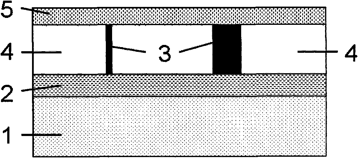
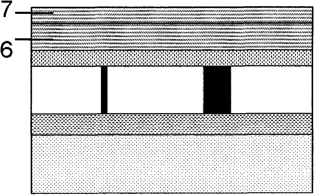
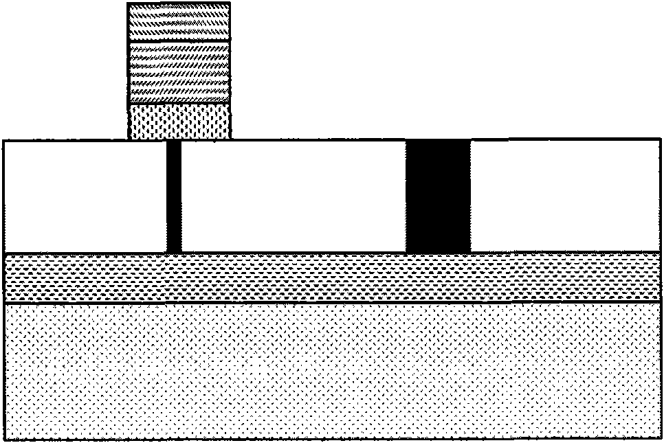
[0046] A phase-change memory unit includes a bottom electrode and a chalcogen compound thin film layer, and also includes a conductive oxide transition layer between the bottom electrode and the chalcogen compound thin film layer. Wherein, the melting point of the conductive oxide transition layer material is 600°C-2500°C; the thermal conductivity is 0.1-120W / mK.

[0047] The material of the conductive oxide transition layer should have high thermal stability, at the melting point of the chalcogenide compound (such as Ge 2 Sb 2 Te 5 It still maintains its thermal stability at a temperature above the melting point of ~600°C, that is, the transition layer material is required to have a melting point greater than that of the chalcogenide compound. And in the temperature range between room temperature and the melting point of the chalcogenide compound, the basic properties of the film of this material, that is, the physical properties (resistivity, film thickness, film roughness...

Embodiment 2

[0063] Adopt the same technical scheme as Example 1, the difference is that the material of the conductive oxide transition layer prepared in step (1) is changed to LaSrCoO 3 , LaSrMnO 3 , SrRuO 3 , CaRuO 3 and other materials, or Nb-doped SrTiO 3 , can also achieve the same technical effect. The melting point of these conductive oxide materials is 600°C-2500°C; the thermal conductivity is 0.1-120W / mK. Wherein, these materials and their preparation methods are well-known techniques of those skilled in the art, and the innovation of the present invention is not these materials themselves, so details will not be repeated here.

Embodiment 3

[0065] Adopt the same technical scheme as embodiment one, the difference is that the material of the chalcogenide film layer described in step (2) is replaced by Sb 2 Te 3 、 Ge 1 Sb 4 Te 7 or Ge 1 Sb 2 Te 4 One of them, or a compound modified by doping one or two elements of N, O, Si, Sn, Ag or In.


PUM

PropertyMeasurementUnit
Melting pointaaaaaaaaaa
Thermal conductivityaaaaaaaaaa
Thicknessaaaaaaaaaa

Abstract

The invention provides a conductive oxide transition layer and a phase-changing memory unit with same and the phase-changing memory unit comprises a conductive oxide transition layer between a bottom electrode and a chalcogenide film with the thickness controlled to 2-10nm. The conductive oxide transition layer of the invention has good thermal stability, has good adhesivity to medium material, chalcogenide and W electrode, has lower thermal conductivity so that the heat efficiency of devices can be effectively improved and has better electroconductibility so that a big capacitor can be avoided to introduce. By planting the new conductive oxide transition layer material, the heating efficiency of devices can be improved effectively so that the operative voltage can be reduced, the diffusion of Sb and Te elements to the direction of the bottom W electrode in the phase-changing material can be avoided, and the chemical reaction between the transition layer and the bottom W electrode and the phase-changing material can not be performed, thus ensuring the consistency of the operation in the duty-cycle operation of devices and increasing the device life of devices.

Description

technical field [0001] The invention relates to the structure, preparation method and material of the phase change memory, in particular to a conductive oxide transition layer for improving the thermal efficiency of the phase change memory and reducing the power consumption of the phase change memory unit and its realization method. The invention belongs to the field of microelectronic nano material and device preparation. Background technique [0002] Phase Change Memory (Phase Change Memory, PCM) is a new type of semiconductor memory, which uses chalcogenide compounds as storage media, and uses electric energy (heat) to make materials change between crystalline (low resistance) and amorphous (high resistance) The mutual conversion between them realizes the writing and erasing of information, and the reading of information is realized by measuring the change of resistance. Compared with a variety of semiconductor storage technologies currently available, including conventi...

Claims


Application Information

Patent Timeline
IPC IPC(8): H01L45/00G11C11/56
Inventor 宋三年宋志棠刘波吴良才封松林
Owner SHANGHAI INST OF MICROSYSTEM & INFORMATION TECH CHINESE ACAD OF SCI
Why Eureka
Try Eureka