TFT-LCD array substrate and manufacturing method thereof

A technology of an array substrate and a manufacturing method, which is applied in the field of thin-film transistor liquid crystal display and its manufacturing, can solve the problems of affecting the comprehensive display brightness of TFT-LCD, high design complexity, and reducing the aperture ratio, so as to achieve improved electrical characteristics and good parameter characteristics , the effect of increasing the aperture ratio

Inactive Publication Date: 2010-01-06
BOE TECH GRP CO LTD +1
View PDF0 Cites 11 Cited by
  • Summary
  • Abstract
  • Description
  • Claims
  • Application Information

AI Technical Summary

Problems solved by technology

[0004] The core functional device of the TFT-LCD array substrate is the thin film transistor, and the electrical characteristics of the thin film transistor such as threshold voltage (Vth), turn-on current (Ion), leakage current (Ioff), and migration speed (Mob) are very important to determine The display effect of TFT-LCD, therefore, in the prior art, the optimization of the electrical characteristics of thin film transistors is generally achieved through the design of TFT shape and structure and the selection of suitable materials, such as a suitable width-to-length ratio W / L (source electrode and drain electrode The relative distance is the length L of the TFT channel region, the length of the effective opposite region of the source electrode and the drain electrode is the width W of the TFT channel region, and the width-to-length ratio W / L affects the turn-on current), suitable semiconductor layer formation conditions (affects Mobility), suitable gate insulating layer thickness (affects storage capacitance), suitable electrode width and thickness (determines signal attenuation degree), etc., and the display effect of TFT-LCD has a lot to do with other factors , such as aperture ratio, box thickness, driving voltage value, and public voltage value, etc. These factors restrict each other, and they affect the whole body. The improvement of a certain effect sometimes affects other aspects.
For example, in order to increase the refresh frequency of the scanning voltage, it is usually required to increase the turn-on current. At this time, you can choose to increase the driving voltage or increase the width-to-length ratio W / L, but the electrical impact caused by increasing the driving voltage will lead to the display Other problems, while changing the width-to-length ratio W / L requires precise control of the process, which often leads to problems such as a decrease in yield
For another example, in order to obtain a good voltage retention effect, it is necessary to increase the storage capacitor, that is, to increase the overlapping area of ​​the electrodes forming the storage capacitor, but this will inevitably reduce the aperture ratio and affect the overall display brightness of the TFT-LCD.
[0005] Therefore, the structural design of the TFT-LCD array substrate in the prior art requires comprehensive coordination of various factors. Not only is the design complexity high, but there are still corresponding defects in the comprehensive and coordinated structure. The electrical characteristics of the formed thin film transistor are: The thickness of the gate electrode is around, the thickness of the gate insulating layer is The length L of the TFT channel region is about 4 μm, and the width W of the TFT channel region is about 25 μm. There are still defects such as small aperture ratio and long response time.

Method used


Image

  • TFT-LCD array substrate and manufacturing method thereof
  • TFT-LCD array substrate and manufacturing method thereof
  • TFT-LCD array substrate and manufacturing method thereof

Examples


Embodiment Construction

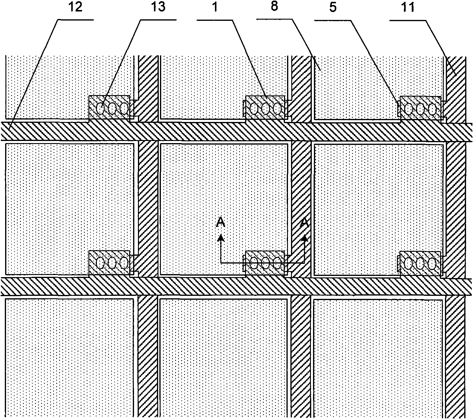
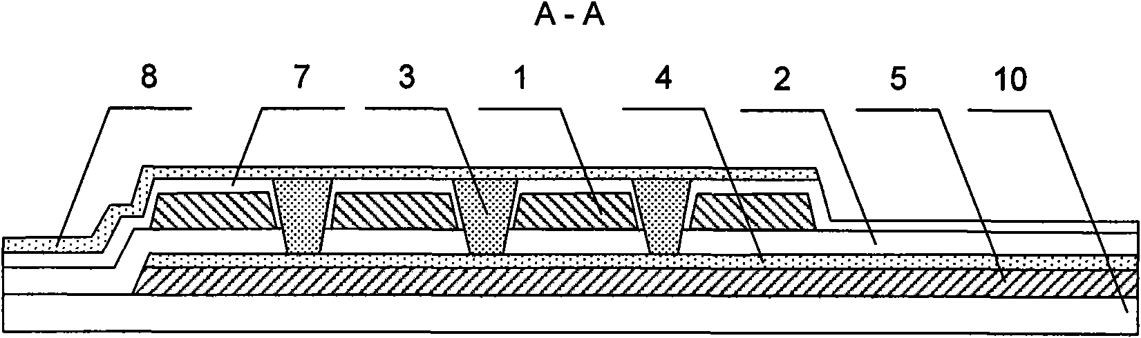
[0044] figure 1 It is a plan view of the first embodiment of the TFT-LCD array substrate of the present invention, figure 2 for figure 1 A cross-sectional view in the direction of A-A. Such as figure 1 , figure 2 As shown, the TFT-LCD array substrate of the present embodiment includes data lines 11, gate lines 12, thin film transistors (TFTs) and pixel electrodes 8, and gate lines 12 and data lines 11 crossing each other define several pixel regions. A TFT is formed at the position, and the pixel electrode 8 is formed in the pixel area and is formed on the uppermost layer away from the substrate. TFT comprises a gate electrode 1, a first insulating layer 2, a semiconductor layer 3, a doped semiconductor layer 4, a source electrode 5 and a second insulating layer 7, the source electrode 5 is formed on a substrate 10, and the doped semiconductor layer 4 is formed on the source electrode 5, the first insulating layer 2 is formed on the doped semiconductor layer 4 and cover...


PUM

PropertyMeasurementUnit
diameteraaaaaaaaaa
widthaaaaaaaaaa

Abstract

The invention relates to a TFT-LCD array substrate and a manufacturing method thereof. The array substrate comprises a grid wire, a data wire, a pixel electrode and a thin film transistor. The array substrate is characterized in that the thin film transistor comprises a grid electrode connected with the grid wire and a source electrode connected with the data wire; at least one through hole is formed on the grid electrode or a through groove is formed on at least one side of the grid electrode; and a semiconductor layer which is connected with the pixel electrode and the source electrode respectively is filled in the through hole or the through groove. The array substrate changes a 'planar type' TFT structure which is universally adopted in the prior art, changes the planar structure into a spatial structure, and has the characteristics of simple and compact structure, good parameter property, simple manufacturing process and the like. The array substrate realizes the effect of increasing the starting current and has certain improvement on other electrical parameters, and the spatial structure of the array substrate reduces the planar size and increases the spatial utilization rate so as to increase the opening ratio.

Description

technical field [0001] The invention relates to a thin film transistor liquid crystal display and a manufacturing method thereof, in particular to a thin film transistor liquid crystal display array substrate and a manufacturing method thereof. Background technique [0002] The main structure of the Thin Film Transistor Liquid Crystal Display (TFT-LCD) includes an array substrate and a color filter substrate that are boxed together and the liquid crystal is sandwiched between them. The liquid crystal molecules are deflected in an orderly manner through voltage control. The light and dark changes of light are generated, and the voltage control is completed by the thin film transistor on the array substrate. [0003] The structure of the prior art bottom-gate TFT-LCD array substrate includes a substrate, a gate electrode formed on the substrate, a gate insulating layer, a semiconductor layer and a doped semiconductor layer formed on the gate electrode, on which a source electr...

Claims


Application Information

Patent Timeline
Patent Type & Authority Applications(China)
IPC IPC(8): G02F1/1362H01L27/12H01L29/786H01L21/84
CPCH01L29/78642
Inventor 高浩然申伟刘华
Owner BOE TECH GRP CO LTD
Why Eureka
Try Eureka