Method for manufacturing body-contact structure of partially depleted SOI MOSFET

A body contact and device technology, which is applied in the field of body contact structure of partially depleted silicon-on-insulator devices, can solve the problems of increased body parasitic capacitance, prolonged body discharge time, unfavorable floating body effect, etc., and achieves reduced body lead-out resistance, Inhibition of floating body effect, inhibition of possession effect

Active Publication Date: 2010-01-06
BEIJING ZHONGKE XINWEITE SCI & TECH DEV
View PDF0 Cites 11 Cited by
  • Summary
  • Abstract
  • Description
  • Claims
  • Application Information

AI Technical Summary

Problems solved by technology

However, an increase in the thickness of the silicon film will increase the source-drain junction depth of the device, which will increase the contact area between the source-drain sidewall and the body region, resulting in an increase in body parasitic capacitance, w

Method used


Image

  • Method for manufacturing body-contact structure of partially depleted SOI MOSFET
  • Method for manufacturing body-contact structure of partially depleted SOI MOSFET
  • Method for manufacturing body-contact structure of partially depleted SOI MOSFET

Examples


Embodiment Construction

[0035] In order to make the objectives, technical solutions, and advantages of the present invention clearer, the following further describes the present invention in detail in conjunction with specific embodiments and with reference to the accompanying drawings.

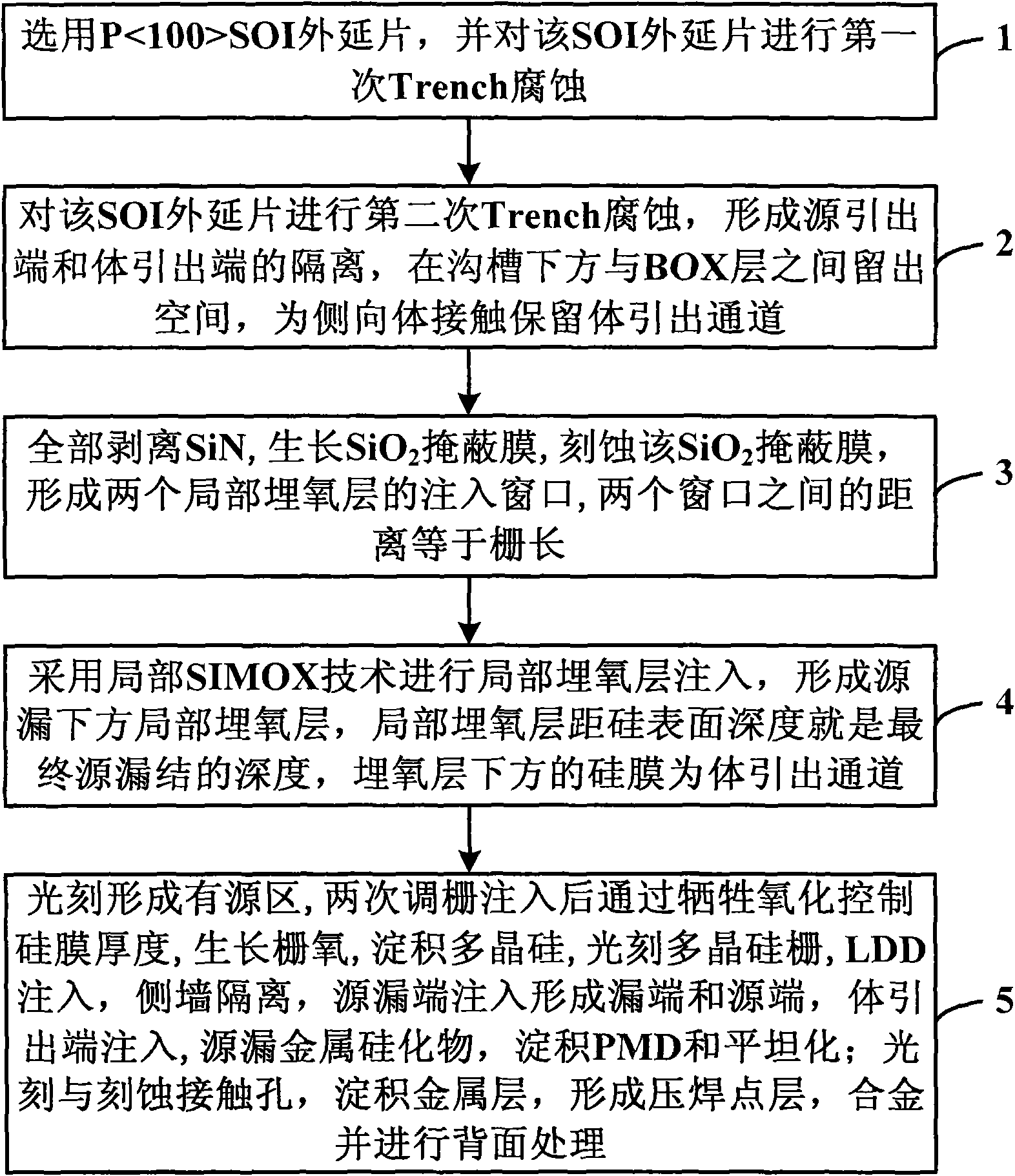
[0036] figure 1 It is a flow chart of the method for manufacturing a body contact structure of a partially depleted SOI device according to the present invention. The specific implementation of the structure of the present invention will be described in detail below with reference to the accompanying drawings.

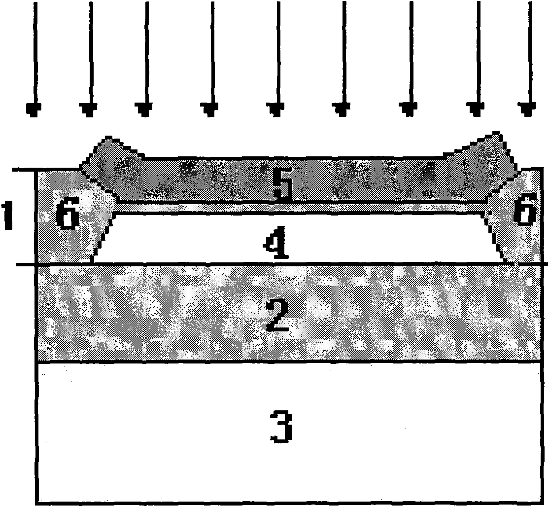
[0037] Step 1, such as figure 2 As shown, select P SOI epitaxial wafer, silicon film (1) thickness of 600nm, BOX layer (2) thickness of 400nm, substrate (3) thickness of 2000nm, gettering oxidation, P-well exposure, P-well (4) injection, injection B+ energy 60KEV, dose 8.5E12, grow SiO 2 Oxide layer, grow SiN (5), etch SiN to form the STI isolation window, perform the first trench etching, the trench reaches th...


PUM


Abstract

The invention discloses a method for manufacturing a body-contact structure of a partially depleted SOI MOSFET, which comprises the following steps: selecting a P<100>SOI epitaxial wafer and subjecting the SOI epitaxial wafer to primary Trench corrosion; performing secondary Trench corrosion to form an isolation layer between a source leading-out end and a body leading-out end and preserving a space between the bottom of a trench and a BOX layer to preserve a body leading-out channel for lateral body contact; stripping SiN completely, growing a SiO2 mask film and etching the SiO2 mask film to form injection windows of two local buried oxide layers; injecting the local buried oxide layers to form local buried oxide layers under source and drain regions; forming an active region by photoetching, performing tuned grid injection twice, controlling the thickness of a silicon film by sacrificial oxidation, growing gate oxide, depositing polysilicon, etching a polysilicon gate, performing LDD injection and side wall isolation, performing source and drain end injection to form a drain end and a source end, performing body leading-out end injection, growing source and drain silicide and performing PMD and planarization; and photoetching and etching contact holes, depositing a metal layer to form a pad layer and alloy, and performing back treatment.

Description

Technical field [0001] The invention relates to a semiconductor device and a manufacturing method thereof, in particular to a method for manufacturing a body contact structure of a partially depleted silicon-on-insulator (SOI) device. Background technique [0002] While SOI technology brings improvements in device and circuit performance, it also inevitably brings adverse effects. The biggest problem is the floating body effect of partially depleted SOI devices. The floating body effect can produce floating body effects such as kink effect, reduced leakage breakdown voltage, and abnormal subthreshold slope, which seriously affects the performance of the device, and even causes the device to fail. [0003] Since the floating body effect has an adverse effect on the performance of the device, the research on how to suppress the floating body effect has always been a hot spot in the research of SOI devices. The solution to the floating body effect is also divided into two categories,...

Claims


Application Information

Patent Timeline
IPC IPC(8): H01L21/336H01L21/84
Inventor 宋文斌毕津顺韩郑生
Owner BEIJING ZHONGKE XINWEITE SCI & TECH DEV
Why Eureka
Try Eureka