Molecular beam epitaxial method for growing non-antiphase domain gallium arsenide film on germanium substrate

A technology of molecular beam epitaxy and anti-phase domain, which is applied in chemical instruments and methods, single crystal growth, crystal growth, etc., and can solve problems such as complex epitaxy process

Inactive Publication Date: 2010-01-13
INST OF SEMICONDUCTORS - CHINESE ACAD OF SCI
View PDF0 Cites 9 Cited by
  • Summary
  • Abstract
  • Description
  • Claims
  • Application Information

AI Technical Summary

Problems solved by technology

This undoubtedly makes the whole epitaxy process more complicated

Method used


Image

  • Molecular beam epitaxial method for growing non-antiphase domain gallium arsenide film on germanium substrate
  • Molecular beam epitaxial method for growing non-antiphase domain gallium arsenide film on germanium substrate
  • Molecular beam epitaxial method for growing non-antiphase domain gallium arsenide film on germanium substrate

Examples


Embodiment Construction

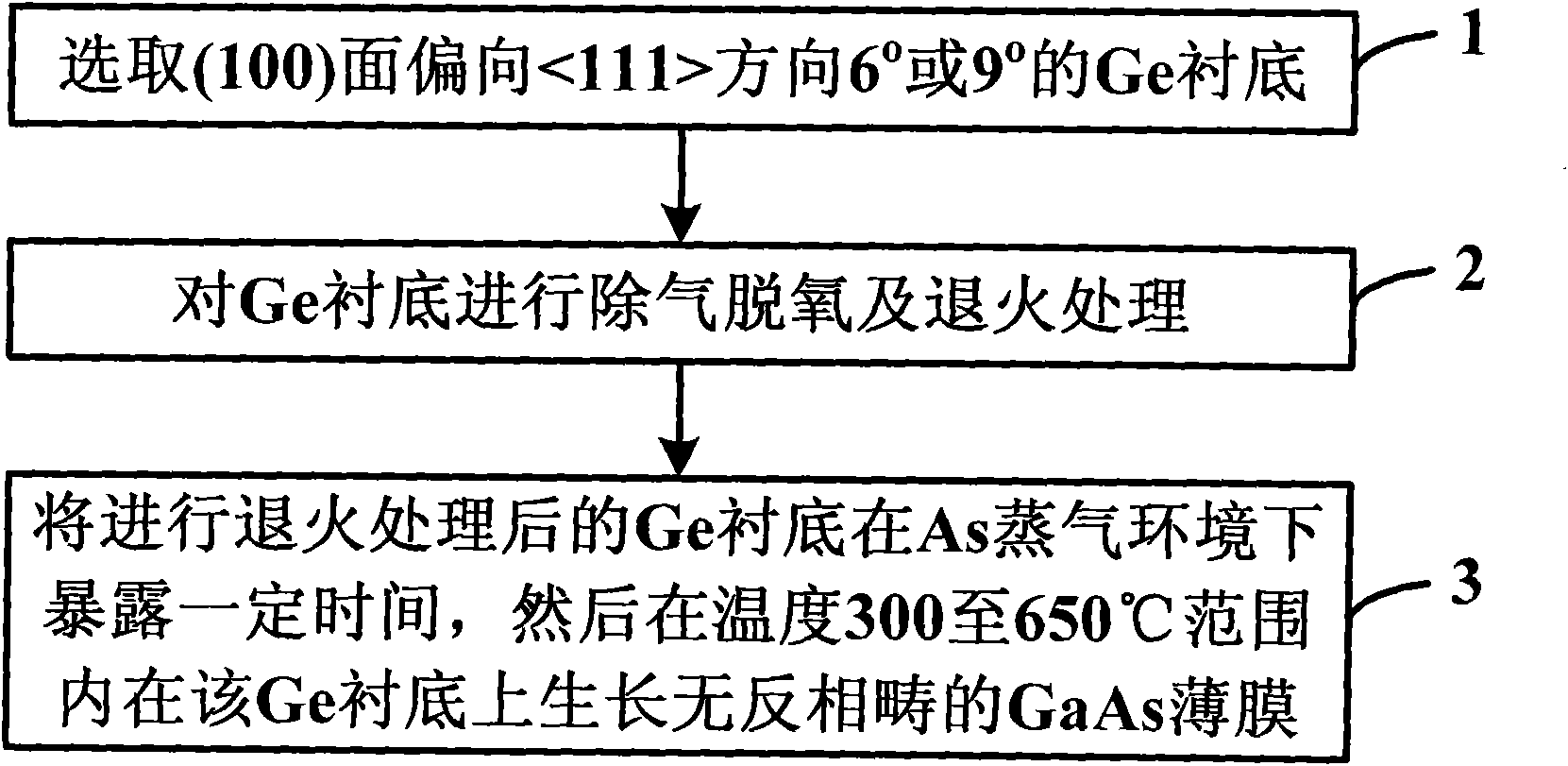
[0024] In order to make the object, technical solution and advantages of the present invention clearer, the present invention will be described in further detail below in conjunction with specific embodiments and with reference to the accompanying drawings.

[0025] Glue the Ge substrate on the sample holder with indium (In), and introduce it into the sample chamber for baking at a temperature of 180 degrees.

[0026] The baked Ge substrate is introduced into the buffer chamber and degassed at 420 degrees, and the atmospheric pressure of the buffer chamber is reduced to 10 -8 When the Torr is below, the degassing is complete.

[0027] The degassed Ge substrate is introduced into the growth chamber, and the temperature of the substrate heater is raised, and the deoxidation and annealing of the sample are performed without As protection. Wherein the annealing temperature ranges from 500 to 700° C., and the annealing time ranges from 5 to 30 minutes.

[0028] During the anneali...


PUM

PropertyMeasurementUnit
thicknessaaaaaaaaaa
surface roughnessaaaaaaaaaa

Abstract

The method discloses a molecular beam epitaxial method for growing a non-antiphase domain gallium arsenide film on a germanium substrate. The method comprises the followings steps of : step one, selecting the Ge substrate of which the (100) plane deviates 6 to 9 degrees from the <111> direction; step two, performing the degassing deoxidation and the annealing treatment of the Ge substrate; and step three, exposing the Ge substrate undergoing the annealing treatment under an environment of As vapor for a period of time, and growing the non-antiphase domain GaAs film on the Ge substrate at a temperature of between 300 and 650 DEG C. Tests show that the surface roughness of the GaAs film grown by the method is only 0.718nm, namely the generation of the antiphase domain is successfully inhibited, and the crystal mass of the film is better than the best result in the present world.

Description

technical field [0001] The invention relates to the technical field of semiconductor materials, in particular to a method for epitaxial growth of polar heterogeneous materials on a non-polar material substrate, in particular to gallium arsenide (GaAs) without anti-phase domains on a germanium (Ge) substrate ) thin film molecular beam epitaxy growth method. Background technique [0002] With the rapid development of global industry and population growth, the demand for energy is increasing, while the reserves of traditional non-renewable energy such as coal, petroleum and other fossil fuels are limited, which makes solar cells appear as a new type of energy in front of people. At the same time, with the continuous development of communication technology, more and more solar cells are required to be used in space technology. Compared with Si cells, high-efficiency GaAs solar cells have become an internationally recognized new generation of space solar cells because of their ...

Claims


Application Information

Patent Timeline
Patent Type & Authority Applications(China)
IPC IPC(8): C30B29/44C30B23/02H01L21/203
Inventor 王鹏飞吴东海吴兵朋熊永华詹峰黄社松倪海桥牛智川
Owner INST OF SEMICONDUCTORS - CHINESE ACAD OF SCI
Why Eureka
Try Eureka