Semiconductor electrode, manufacture method thereof and solar cell containing same

A technology for solar cells and semiconductors, applied in the field of dye-sensitized solar cells, which can solve the problems of low porosity of porous semiconductor layers

Inactive Publication Date: 2010-01-27
BYD CO LTD
View PDF0 Cites 18 Cited by
  • Summary
  • Abstract
  • Description
  • Claims
  • Application Information

AI Technical Summary

Problems solved by technology

[0005] The purpose of the present invention is to overcome the shortcoming of the low porosity of the existing porous semiconductor layer ...

Method used


Image

  • Semiconductor electrode, manufacture method thereof and solar cell containing same
  • Semiconductor electrode, manufacture method thereof and solar cell containing same
  • Semiconductor electrode, manufacture method thereof and solar cell containing same

Examples


preparation example Construction

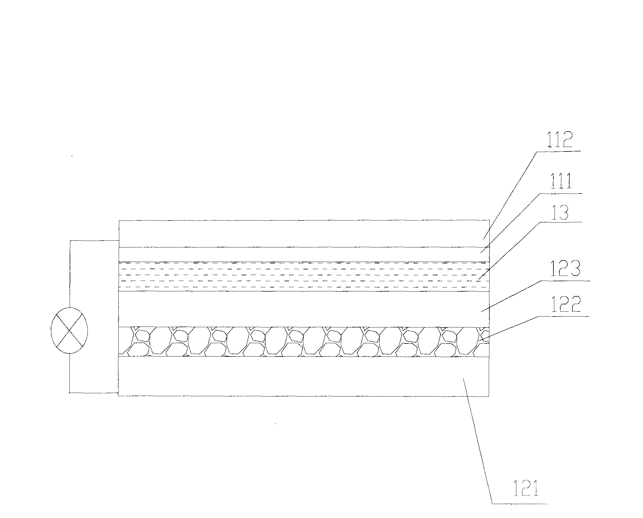
[0016] A method for preparing a semiconductor electrode, the method comprising forming a porous semiconductor layer containing semiconductor particles on a conductive bottom layer, and then forming a dye layer on the porous semiconductor layer, wherein, the method for preparing the porous semiconductor layer includes comprising semiconductor nanoparticles, The slurry of pore-forming agent and dispersant is coated on the conductive bottom layer, and after a period of calcination, during the calcination process, a three-dimensional network porous skeleton with interconnected semiconductor crystal grains is formed, and at the same time, the dispersant is fully volatilized during calcination, and sintered The time is 10-120 minutes, the sintering temperature is 300-600°C, the slurry layer is calcined for a period of time to obtain a solid film, and the conductive bottom layer with the solid film is immersed in a solution that can dissolve the porogen but not dissolve the semiconduct...

Embodiment 1

[0033] This example is used to prepare the semiconductor electrode for a dye-sensitized solar cell provided by the present invention and the dye-sensitized solar cell containing the semiconductor electrode.

[0034] (1) Preparation of semiconductor crystal film precursor solution

[0035] 25 g TiO 2 Granules (particle diameter 30 nm), 0.8 g of CaCO 3 Pore ​​former (pore former and TiO 2 The volume ratio is 1:90), joins in 0.54 gram polyethylene glycol, is configured into slurry, and slurry is put into ball mill (Nanjing University Instrument Factory, model QM-3SP2), is ball milling time 0.5 hour in process condition, ball milling temperature At 25°C, slurry P1 was prepared.

[0036] (2) Preparation of semiconductor electrodes

[0037] The slurry P1 is uniformly coated on a conductive glass coated with a fluorine-doped tin dioxide film with a size of 5 × 2.5 cm (FTO conductive glass with a square resistance of 15 ohms manufactured by Qinhuangdao Yaohua Glass Co., Ltd., and ...

Embodiment 2

[0046] This example is used to prepare the semiconductor electrode for a dye-sensitized solar cell provided by the present invention and the dye-sensitized solar cell containing the semiconductor electrode.

[0047] The dye-sensitized solar cell R2 was prepared in the same manner as in Example 1, except that the slurry P1 was replaced by the slurry P2 prepared as follows, and the volume ratio between the porogen and the semiconductor particles in P2 was 1: 14.

[0048] 25 g TiO 2 Granules (particle diameter 30 nm), 3.2 g of CaCO 3 Pore-forming agent, add 0.58 gram of polyvinylpyrrolidone to be configured into a slurry, the slurry is put into a ball mill (Nanjing University Instrument Factory, model QM-3SP2), and the process conditions are 0.5 hours of ball milling time, and the ball milling temperature is 25°C to obtain a precursor slurry P2.

[0049] The first-stage calcination time is 30 minutes, the calcination temperature is 400°C, the solution used is 200mL, pH=2 nitri...


PUM

PropertyMeasurementUnit
Thicknessaaaaaaaaaa
Diameteraaaaaaaaaa
Thicknessaaaaaaaaaa

Abstract

The invention provides a semiconductor electrode for a dye-sensitized solar cell, comprising a conductive bottom layer, a porous semiconductor layer formed on the conductive bottom layer and a dye layer formed on the porous semiconductor layer, wherein the porosity of the porous semiconductor layer is 40-85% and the thickness of the porous semiconductor layer is 6-20 microns. The invention also provides a preparation method of the semiconductor electrode and the dye-sensitized solar cell containing same, wherein the preparation method comprises the following steps: paving sizing agent which contains semiconductor grains, pore-forming agent and dispersing agent on the conductive bottom layer, calcining the sizing agent to obtain a solid film, putting the solid film in solution to be dipped into pores and obtain a porous solid film, calcining the porous solid film, and forming the porous semiconductor layer on the conductive bottom layer. The porosity of the porous semiconductor layer is high, can improve the absorption load quantity of the dye on the porous semiconductor layer, increases light generated current, and improves opto-electrical conversion rate.

Description

technical field [0001] The invention relates to a semiconductor electrode, a preparation method thereof and a dye-sensitized solar cell containing the semiconductor electrode. Background technique [0002] Swiss Institute of Technology Lausanne Professors and others first proposed the concept of dye-sensitized solar cells in 1991. This solar cell does not require silicon as a raw material, and has the advantages of low cost, simple manufacturing process, and high photoelectric conversion rate compared with silicon solar cells. The emergence of solar cells has brought revolutionary changes in the field of solar cells. [0003] The dye-sensitized solar cell mainly includes a semiconductor electrode, a counter electrode, and an electrolyte between the semiconductor electrode and the counter electrode. The semiconductor electrode includes a conductive bottom layer, a semiconductor layer formed on the conductive bottom layer, and a dye layer formed on the semiconductor layer. ...

Claims


Application Information

Patent Timeline
IPC IPC(8): H01G9/20H01G9/04H01M14/00H01M10/26H01L31/0224H01L31/18H01L31/04H01L51/44H01L51/48H01L51/42
CPCY02E10/542
Inventor 林信平宫清刘倩倩陈炎
Owner BYD CO LTD
Why Eureka
Try Eureka