Laminated film photovoltaic device with plasmon structure and application thereof

A plasmonic and thin-film photovoltaic technology, applied in the direction of photovoltaic power generation, electrical components, electrical solid devices, etc., can solve the problems that the crystal growth speed cannot be too fast, microcrystalline silicon cannot be formed, and the production rate is reduced, so as to reduce the production rate. Cost, increase in element efficiency, effect of increase in absorption length

Inactive Publication Date: 2010-01-27
IND TECH RES INST
View PDF0 Cites 14 Cited by
  • Summary
  • Abstract
  • Description
  • Claims
  • Application Information

AI Technical Summary

Problems solved by technology

Generally, the growth rate of microcrystalline silicon should not be too fast, otherwise microcrystalline silicon cannot be formed, so the growth time of stacked thin film silicon solar cells will be very long, which will increase the cost of materials and reduce the production rate

Method used


Image

  • Laminated film photovoltaic device with plasmon structure and application thereof
  • Laminated film photovoltaic device with plasmon structure and application thereof
  • Laminated film photovoltaic device with plasmon structure and application thereof

Examples


Embodiment Construction

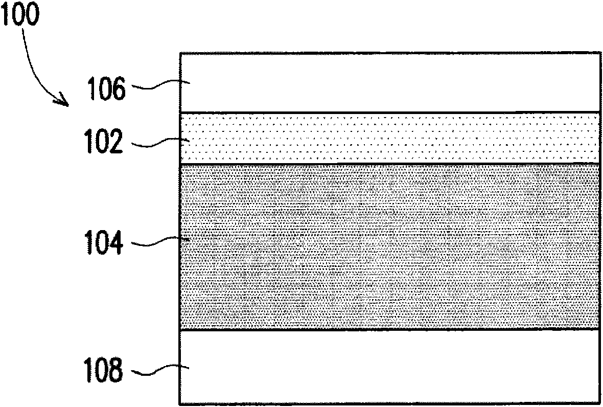
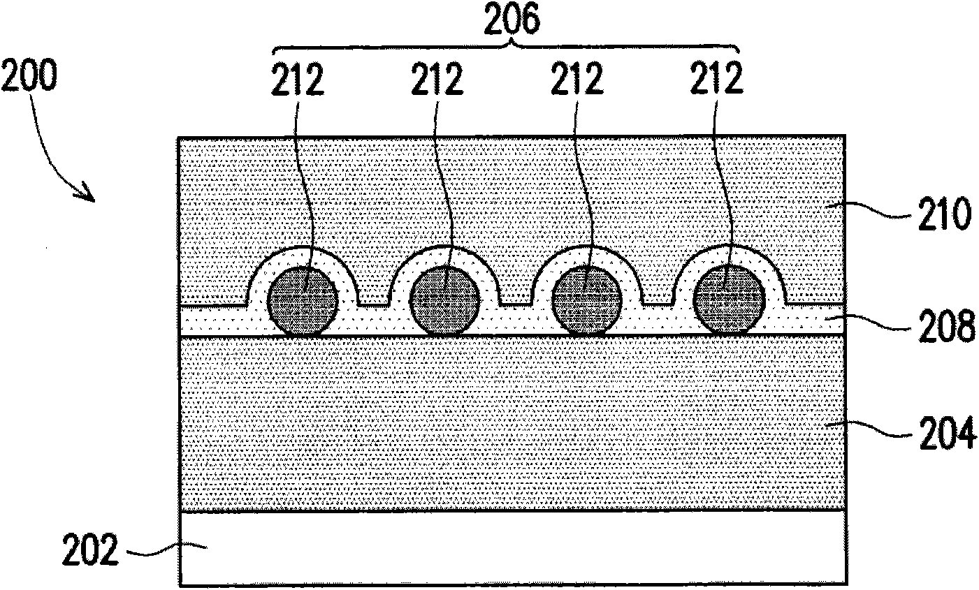
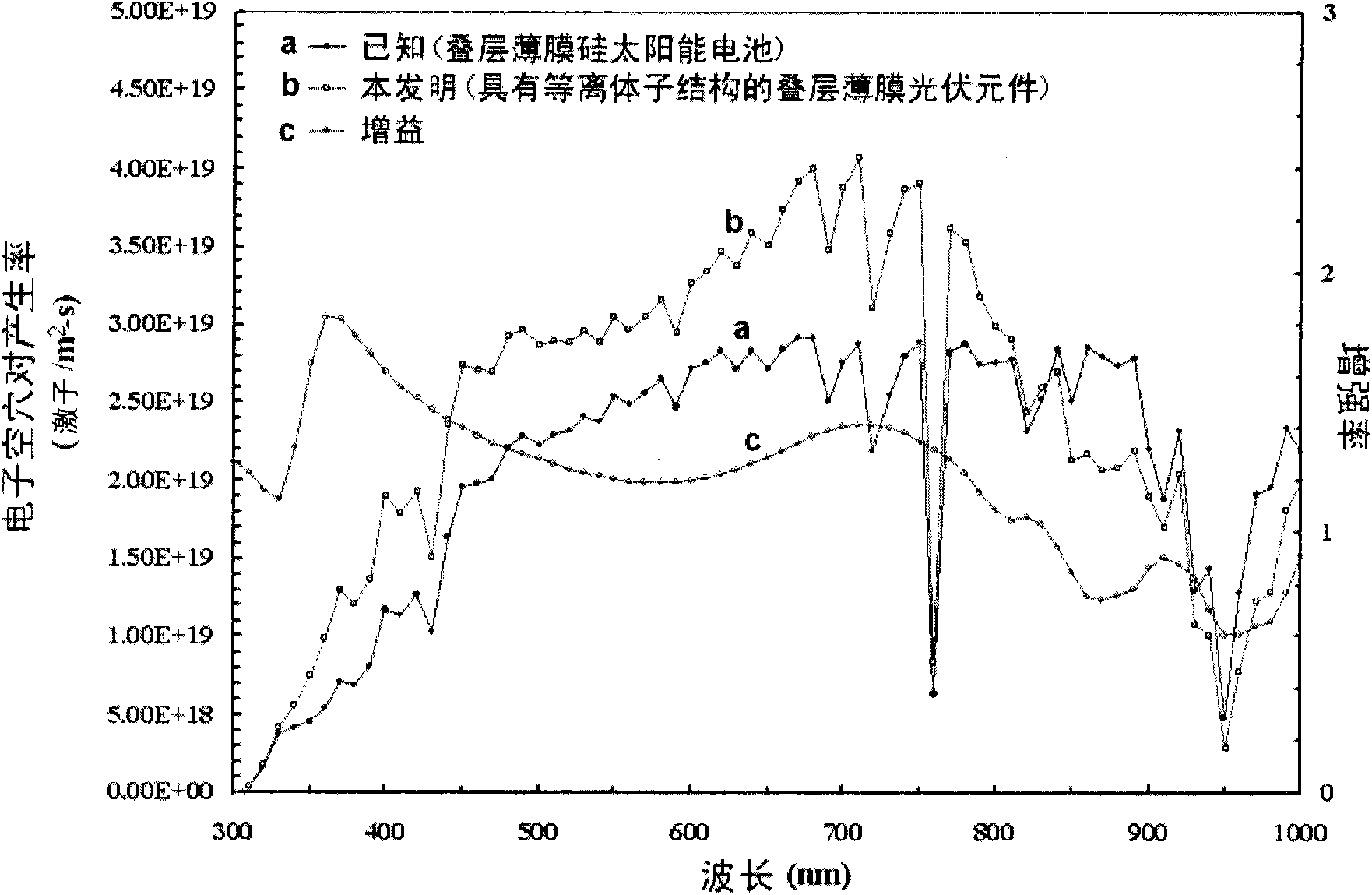
[0036] Plasmons are light or high-frequency electromagnetic waves interacting with metal free electrons, resulting in electron charge density oscillations. When resonance conditions occur, such plasmonic materials will produce extremely high extinction coefficients (extinction) and High-density strong near-field with very special optical properties. According to the Mie scattering theory, the extinction coefficient of metal ball particles with a size of more than 100 nanometers mainly comes from the scattering of the ball, and the heat loss caused by absorption is much lower than the contribution of scattering. This scattering characteristic is related to the material, size and shape of the metal particles, which will cause light to travel in different directions due to different wavelengths, and effectively control the behavior of metal particles, which will help the application of thin-film silicon solar cell light confinement technology . The present invention utilizes the...


PUM

PropertyMeasurementUnit
Particle sizeaaaaaaaaaa

Abstract

The invention relates to a laminated film photovoltaic device with a plasmon structure and application thereof. The laminated film photovoltaic device with the plasmon structure comprises a metal electrode, a low band gap photoelectric conversion layer, a nanometer metal particle plasmon structural layer, a high band gap photoelectric conversion layer and a transparent conductive film, wherein the low band gap photoelectric conversion layer is positioned on the metal electrode; the nanometer metal particle plasmon structural layer is positioned on the low band gap photoelectric conversion layer, and comprises nanometer metal particles of which the particle size is between 100 and 200nm; the high band gap photoelectric conversion layer is positioned on the nanometer metal particle plasmon structural layer; and the transparent conductive film is positioned on the high band gap photoelectric conversion layer. The laminated film photovoltaic device with the plasmon structure can reduce the overall thickness of the device and improve the generation rate of light current.

Description

technical field [0001] The present invention relates to a laminated thin film photovoltaic device, and in particular to a laminated thin film photovoltaic device with a plasmon (also called plasmon, plasmon) structure. Background technique [0002] Due to the expected decrease in oil production in the future, people began to pay attention to clean solar energy. Therefore, the demand for silicon solar cells, which is the most mass-produced and commercialized, has greatly increased, resulting in a serious shortage of raw materials for silicon substrates, and the price has also risen. Therefore, thin-film silicon solar cells formed by film coating have a promising prospect because they are not restricted by a limited substrate and can be conveniently used on different building materials. [0003] Generally, thin-film silicon solar cells are based on a p-i-n single-layer junction structure, and the photocurrent generation mainly comes from the undoped intrinsic layer (i layer), ...

Claims


Application Information

Patent Timeline
IPC IPC(8): H01L31/04H01L51/42H01G9/20H01M14/00H01L31/0445
CPCY02E10/50
Inventor 朱仁佑陈春弟汪天仁阙铭宏
Owner IND TECH RES INST
Why Eureka
Try Eureka