Method for electric discharge machining of micronanometer three-dimensional structure of nanowire or nanotube and system thereof

A technology of electric discharge machining and three-dimensional structure, which is applied in the direction of nanostructure manufacturing, microstructure technology, microstructure device, etc., can solve the problems of difficult chip removal, microstructure size reduction, etc., and achieve the goal of solving chip removal problems and enriching technical methods Effect

Inactive Publication Date: 2012-01-25
TIANJIN UNIV
View PDF2 Cites 2 Cited by
  • Summary
  • Abstract
  • Description
  • Claims
  • Application Information

AI Technical Summary

Problems solved by technology
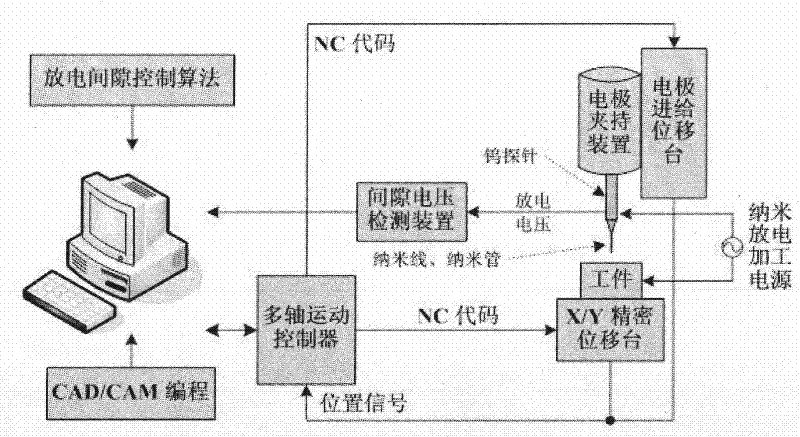
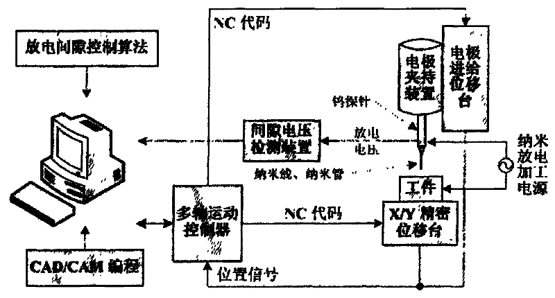
At the same time, because the size of the processed structure is too small, it is difficult to remove chips by using external flushing, which makes the problem of chip removal more prominent in the EDM process, thus restricting the further reduction of the size of the microstructure

Method used


Image

  • Method for electric discharge machining of micronanometer three-dimensional structure of nanowire or nanotube and system thereof
  • Method for electric discharge machining of micronanometer three-dimensional structure of nanowire or nanotube and system thereof
  • Method for electric discharge machining of micronanometer three-dimensional structure of nanowire or nanotube and system thereof

Examples


Embodiment Construction

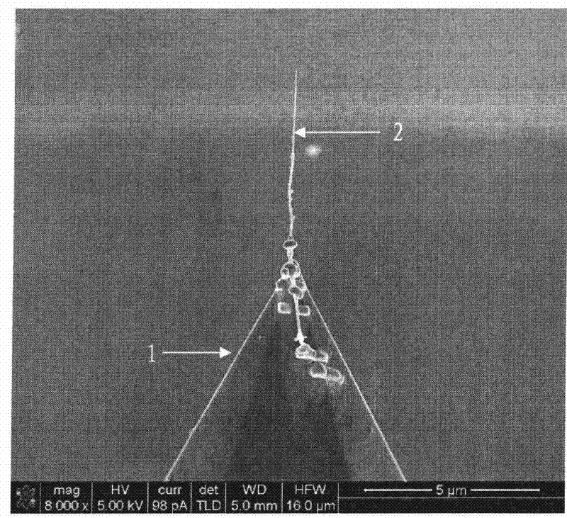
[0020] The present invention uses nanowires and nanotubes as electrodes for nano-discharge processing to process micron and nanoscale complex three-dimensional structures, and the nanowires and nanotubes used as electrodes need to meet the following conditions:

[0021] Nanowires and nanotubes need to have good electrical and thermal conductivity and mechanical properties. For example, the melting point of carbon nanotubes is the highest among known materials at present, and it is not easy to be corroded by heat in electric discharge machining; secondly, the molecular structure of carbon nanotubes is stable and has high thermal stability; thirdly, the structure of carbon nanotubes It has the same sheet structure as graphite, so it has good electrical properties. At the same time, carbon nanotubes have high heat exchange along the tube axis, which is good for heat dissipation during processing; finally, carbon nanotubes have good mechanical properties, and their tensile strength...


PUM

PropertyMeasurementUnit
tensile strengthaaaaaaaaaa

Abstract

The invention belongs to the technical field of micronanometer manufacturing, relating to a method for electric discharge machining of micronanometer three-dimensional structure of a nanowire or a nanotube, comprising: (1) sticking a conductive nanowire or nanotube to a tungsten tip; (2) putting an electrode clamping device onto a displacement table, and controlling the movement of the displacement table via a multi-axis motion controller; (3) putting conductive material workpieces to an X / Y precision displacement table, and controlling the movement of the X / Y precision displacement table by the multi-axis motion controller; (4) connecting the cathode of a pulse power supply to the tungsten tip, and connecting the anode to the workpiece; (5) using an industrial personal computer to send orders to the multi-axis motion controller, controlling the displacement table provided with the electrode clamping device, providing working voltage for electric discharge machining by the pulse powersupply, collecting electric discharge gap voltage by a gap voltage detection device, and controlling the movement of an electrode feeding displacement table by the industrial personal computer according to gap voltage. The invention ensures that the size of electric discharge machining reaches the micrometer level and the nanometer level and simultaneously solves the problem of chip removal in the machining process.

Description

technical field [0001] The invention belongs to the technical field of micro-nano manufacturing, and relates to a method and system for electric discharge machining of a micro-nano three-dimensional structure. Background technique [0002] As one of the special processing technologies, electrical discharge machining has been widely used in industry. With the miniaturization of products, the research on processing technology and methods of micro-nano three-dimensional structure has become one of the main topics in the field of manufacturing. According to different processing principles, the processing of micro-nano three-dimensional structures can be divided into two categories: traditional mechanical processing and special processing. In traditional mechanical processing, due to the existence of macroscopic cutting force, there are phenomena such as stress and heat in the processing process. In micro- and nano-scale processing, it is difficult to control the processing accu...

Claims


Application Information

Patent Timeline
Patent Type & Authority Patents(China)
IPC IPC(8): B82B3/00B81C1/00B81C5/00
Inventor 房丰洲王庆祎徐宗伟胡小唐
Owner TIANJIN UNIV
Why Eureka
Try Eureka