White-light organic electroluminescence device of organic micromolecule multidoped luminescent layer and manufacturing method thereof
A technology of electroluminescent devices and light-emitting layers, which is applied in the fields of electric solid-state devices, semiconductor/solid-state device manufacturing, electrical components, etc., and can solve problems such as simultaneous co-doping of multiple materials
- Summary
- Abstract
- Description
- Claims
- Application Information
AI Technical Summary
Problems solved by technology
Method used
Image
Examples
Embodiment 1
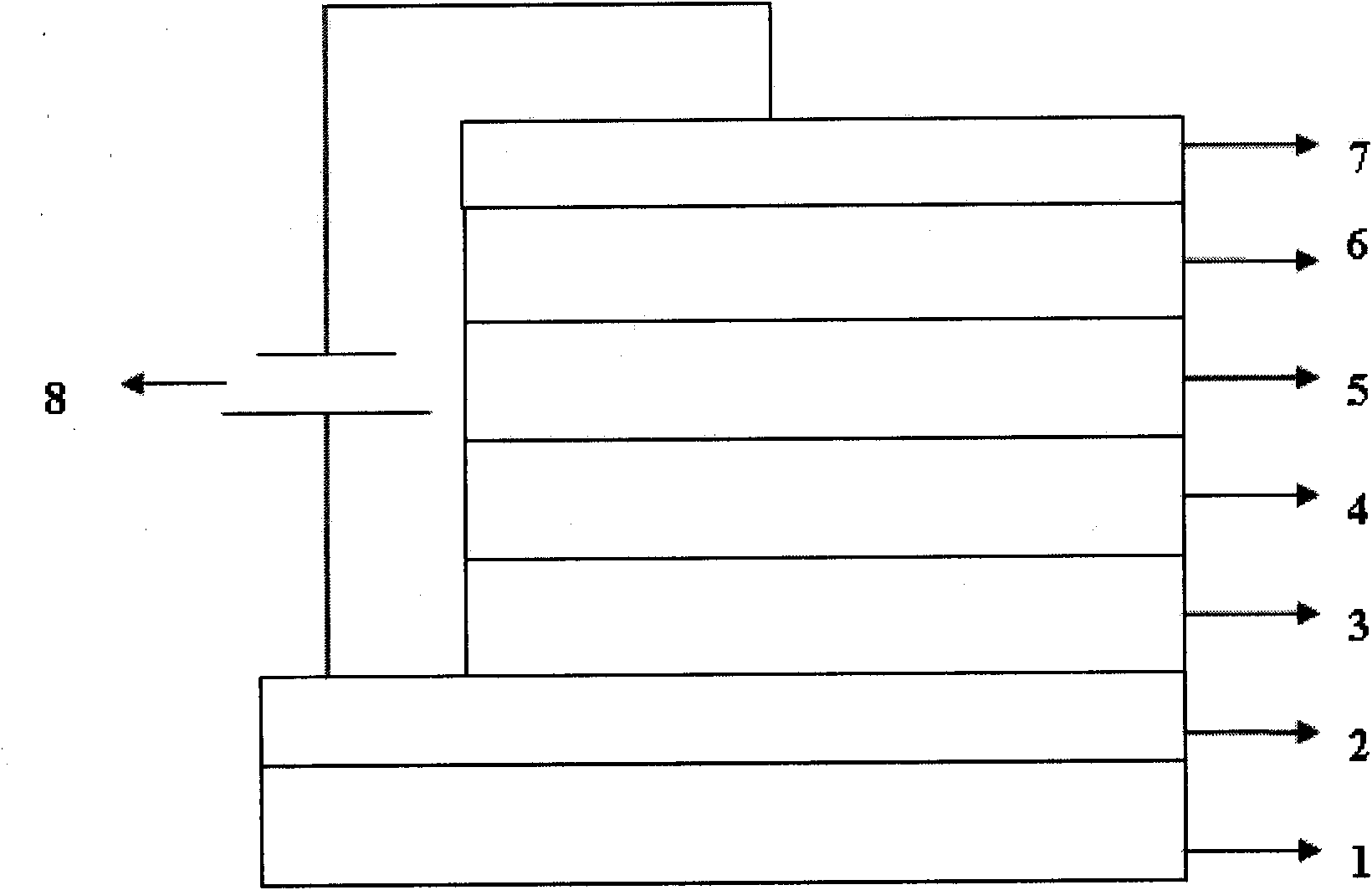
[0043] now refer to figure 1 , the electroluminescent device according to the first embodiment of the present invention has the following structure:
[0044] ITO(100nm) / PVK:F4-TCNQ(40nm) / DPVBi:TPD:Rubrene:DCJTB(40nm) / BCP(10nm) / Alq 3 (30nm) / LiF(0.6nm) / Al(80nm)
[0045] A certain amount of PVK doped with F4-TCNQ on ITO (this example doping concentration is 5%) is the hole-transport layer; continue to spin-coat on it with DPVBi as the blue light-emitting material and the host material after the drying treatment, The hole transport material TPD (diphenylarylamine) is blended with a mixture of orange dye Rubrene and red dye DCJTB to obtain a light-emitting layer with a film thickness of 40nm; after drying, it is placed in a vacuum chamber to evaporate holes to block layer and electron transport layer, and Al combined cathode. In this embodiment, the TPD concentration of the light-emitting layer is 40%, the Rubrene doping concentration is 0.15%, and the DCJTB doping concentration...
Embodiment 2
[0048] now refer to figure 1 , the electroluminescent device according to the second embodiment of the present invention has the following structure:
[0049] ITO(100nm) / PVK(40nm) / DPVBi:TPD:Rubrene:DCJTB(40nm) / BCP(10nm) / Alq 3 (30nm) / LiF(0.6nm) / Al(80nm)
[0050] After the preparation method of the device is the same as that of the above embodiment 1, the test is carried out, and the highest brightness of the device can be achieved, and the efficiency is above 4.0 cd / A.
[0051] The luminance-voltage curve of the organic electroluminescent device of this embodiment 2 is as follows Figure 5 , the color coordinates change with the voltage as Image 6 .
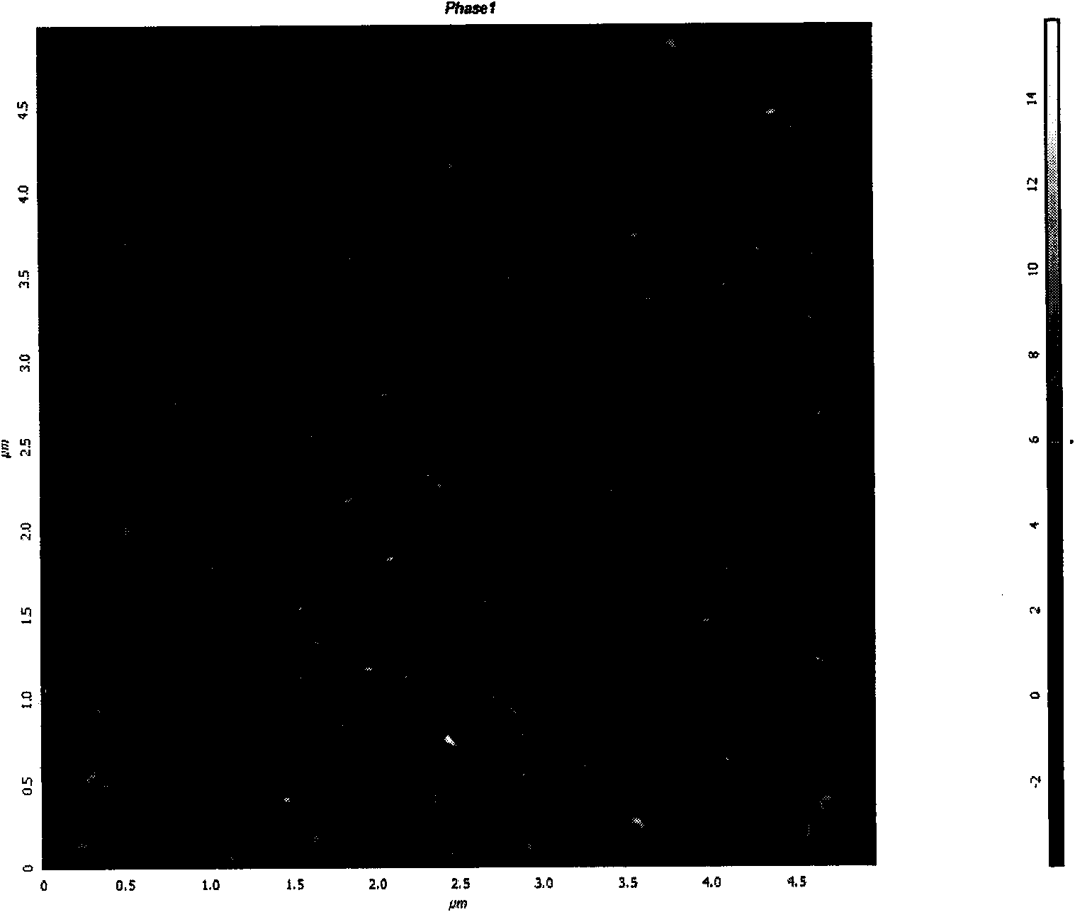
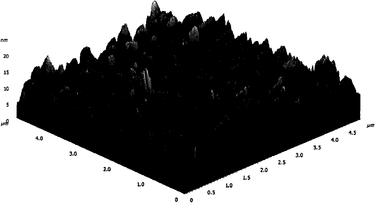
[0052] The spin-coated organic small molecule multi-doped light-emitting layer (DPVBi:TPD (40%):Rubrene:DCJTB) used in the embodiment 1-2 of the present invention has a phase diagram, surface morphology and surface morphology of a separate DPVBi on PVK Appearance AFM diagram White organic electroluminescent device brightness...
PUM
| Property | Measurement | Unit |
|---|---|---|
| Thickness | aaaaa | aaaaa |
| Film thickness | aaaaa | aaaaa |
| Film thickness | aaaaa | aaaaa |
Abstract
Description
Claims
Application Information


