Manufacturing method of light emitting diode (LED) based on inversed roughened surface Gan-base vertical structure

A technology of light-emitting diodes and vertical structures, applied in electrical components, circuits, semiconductor devices, etc., can solve the problems of low light extraction efficiency, sapphire substrate, low insulation and low thermal conductivity, and low efficiency of GaN-based light-emitting devices, so as to improve the internal quantum efficiency , high luminous efficiency, and the effect of improving the quality of the crystal lattice

Active Publication Date: 2010-03-03
XIAMEN SANAN OPTOELECTRONICS TECH CO LTD
View PDF0 Cites 10 Cited by
  • Summary
  • Abstract
  • Description
  • Claims
  • Application Information

AI Technical Summary

Problems solved by technology

[0003] In order to comprehensively solve the above-mentioned problems of low efficiency of GaN-based light-emitting devices caused by the high-density defects, low light extraction efficiency and low thermal conductivity of the sapphire substrate of GaN-based epitaxy using sapphire as the growth substrate, the present invention innovatively proposes a Fabrication method of GaN-based vertical structure light-emitting diode with inverted rough surface

Method used


Image

  • Manufacturing method of light emitting diode (LED) based on inversed roughened surface Gan-base vertical structure
  • Manufacturing method of light emitting diode (LED) based on inversed roughened surface Gan-base vertical structure
  • Manufacturing method of light emitting diode (LED) based on inversed roughened surface Gan-base vertical structure

Examples


Embodiment Construction

[0032] The present invention will be further described below in conjunction with the accompanying drawings and embodiments.

[0033] A method for manufacturing a GaN-based vertical structure light-emitting diode based on an inverted rough surface, the process of which is implemented as follows:

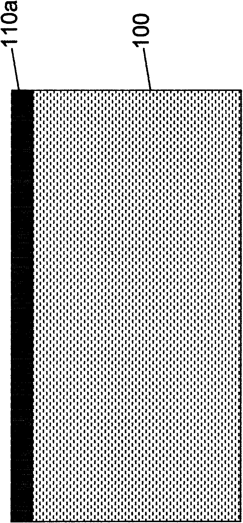
[0034] like Figure 1a As shown, an undoped GaN material layer 110a with a thickness of 2 microns is epitaxially grown on a sapphire substrate 100 by MOCVD method;

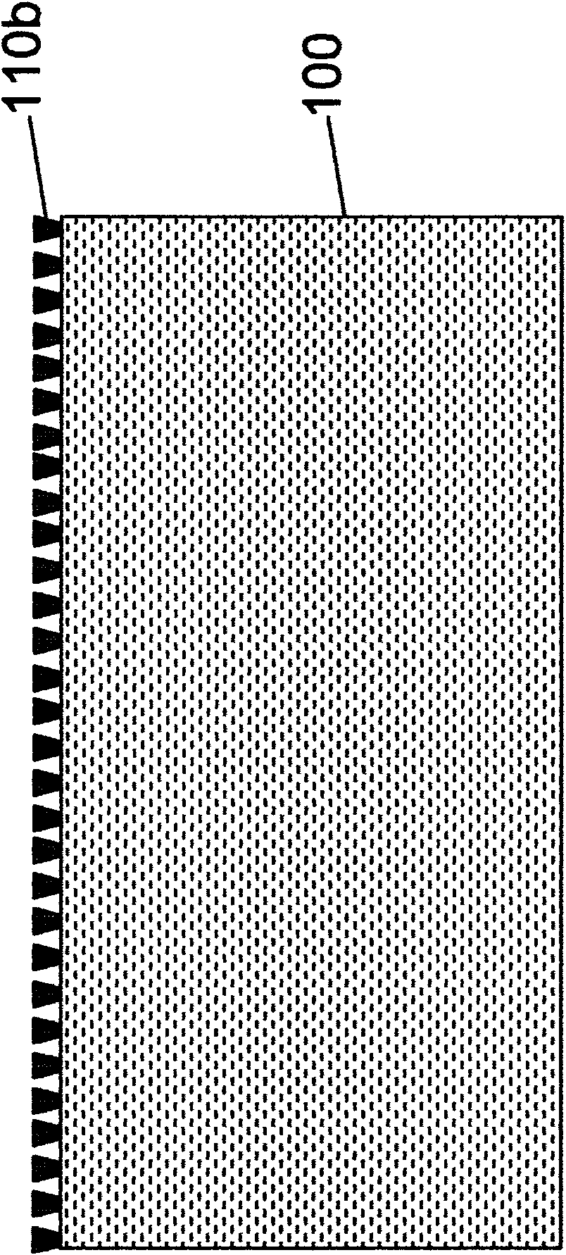
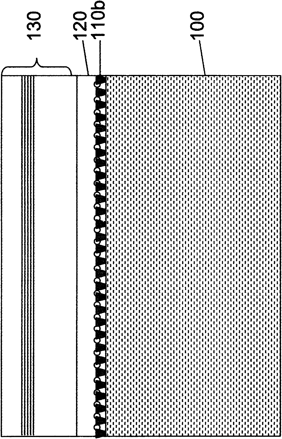
[0035] like Figure 1b As shown, the wafer prepared in step 1 is immersed in a high-temperature molten KOH solution. The temperature of the KOH solution is heated to 280° C., and the etching time lasts for 10 minutes. The undoped GaN material layer 110a is anisotropic in the high-temperature molten KOH solution. Etching forms several inverted hexagonal rhomboid grooves, the opening diameter of the hexagonal rhomboid grooves is between 1 micron and 3 microns, and a discontinuous gap is formed between the bottom of the un...


PUM

PropertyMeasurementUnit
thicknessaaaaaaaaaa
thicknessaaaaaaaaaa
thicknessaaaaaaaaaa

Abstract

The invention discloses a manufacturing method of an LED based on an inversed roughened surface Gan-base vertical structure, which comprises the following steps: growing a non-doped GaN material layeron a spphire substrate by adopting an MOCVD method; and continuously growing an LED extension illuminating material layer after carrying out anisotropic etching on the non-doped GaN material layer. After etching, the bottom surface of the non-doped GaN material layer and spphire form a discontinuous bonding interface, on the one hand, the LED extension stress of the release part improves the quality of an LED extension crystal lattice and improves the internal quanntum efficiency; and on the other hand, after the spphire substrate is removed, the discontinuous bonding interface naturally inverses into a roughened light emergent surface and improves the light collection efficiency of LED devices, therefore, the LED with GaN-based vertical structure has higher illuminating efficiency and isparticularly suitable for heavy current drive.

Description

technical field [0001] The invention relates to a method for manufacturing a GaN-based semiconductor light-emitting device, in particular to a method for manufacturing a GaN-based vertical structure light-emitting diode based on an inverted rough surface. Background technique [0002] Because sapphire substrates are easy to manufacture and low in price, most gallium nitride (GaN)-based epitaxial materials are grown on sapphire substrates at present. However, the GaN-based epitaxy using sapphire as the growth substrate has the following disadvantages: 1. There is a large lattice mismatch and thermal mismatch between the GaN-based semiconductor material and the sapphire substrate, resulting in the GaN-based epitaxy material High defect density (10 8 -10 10 cm -2 ), so that most of the electrical input is converted to non-radiative recombination. In order to solve this problem, technologies such as lateral epitaxial growth (ELOG) and patterned sapphire substrate (PSS) have ...

Claims


Application Information

Patent Timeline
Patent Type & Authority Applications(China)
IPC IPC(8): H01L33/00
Inventor 林雪娇吴志强潘群峰叶孟欣黄慧君
Owner XIAMEN SANAN OPTOELECTRONICS TECH CO LTD
Why Eureka
Try Eureka