

Method for molding multi-layer plate-type array-structure ceramic filter
A technology of ceramic filter and array structure, which is applied in waveguide type devices, stone processing equipment, laser welding equipment, etc. Production schedule and efficiency, ensure accuracy and accuracy, and ensure the effect of electrical performance
Inactive Publication Date: 2010-03-17
CHENGDU HONGMING ELECTRONICS CO LTD
View PDF2 Cites 11 Cited by
- Summary
- Abstract
- Description
- Claims
- Application Information
AI Technical Summary
Problems solved by technology
The disadvantages of the drilling and punching method are: 1. Punching through a punching machine or drilling with a drilling machine, the pressure of the punching machine or drilling machine is high, which will cause cracking and damage to the inner hole and outer contour edge of the ceramic filter after blanking, which will affect the filter. Electrical properties. At the same time, the inner hole and outer contour of the filter after blanking are not smooth, and there is residual film material, which makes the filter electrodes unable to be drawn out, thus affecting the filter capacitance; 2. Alignment by mold punching or drilling The precision is not high, and it is easy to cause deviation and dislocation of the inner hole and outer contour, which will affect the electrical performance and assembly of the filter; 3. The mold production cycle is long and the procedure is complicated. One product corresponds to a pair of molds. Since there are many types of filters, this method Not suitable for variety diversification needs
Method used
View moreImage
Smart ImageViewing Examples

Examples
Embodiment approach
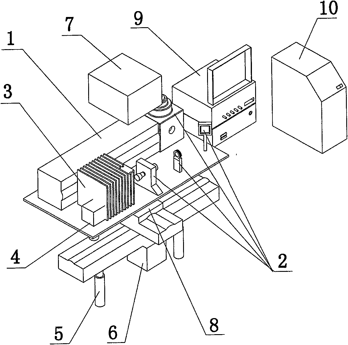
[0031] In the third embodiment of the present invention, other method steps are the same as those of the foregoing embodiments, the difference being that the ceramic green body placed on the workbench for laser drilling and cutting is a raw material film, and after printing, it undergoes the process described in the foregoing embodiments. After the laser drilling and cutting molding process steps, after multi-layer overlapping, warm isostatic pressing, and finally row bonding and sintering into porcelain.
Login to View More PUM
| Property | Measurement | Unit |
|---|---|---|
| size | aaaaa | aaaaa |
| thickness | aaaaa | aaaaa |
Abstract
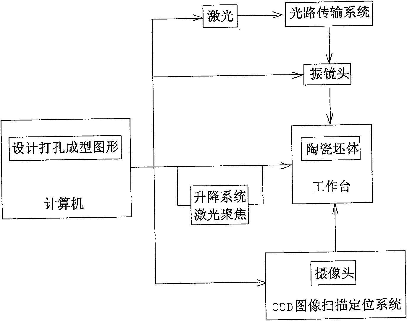
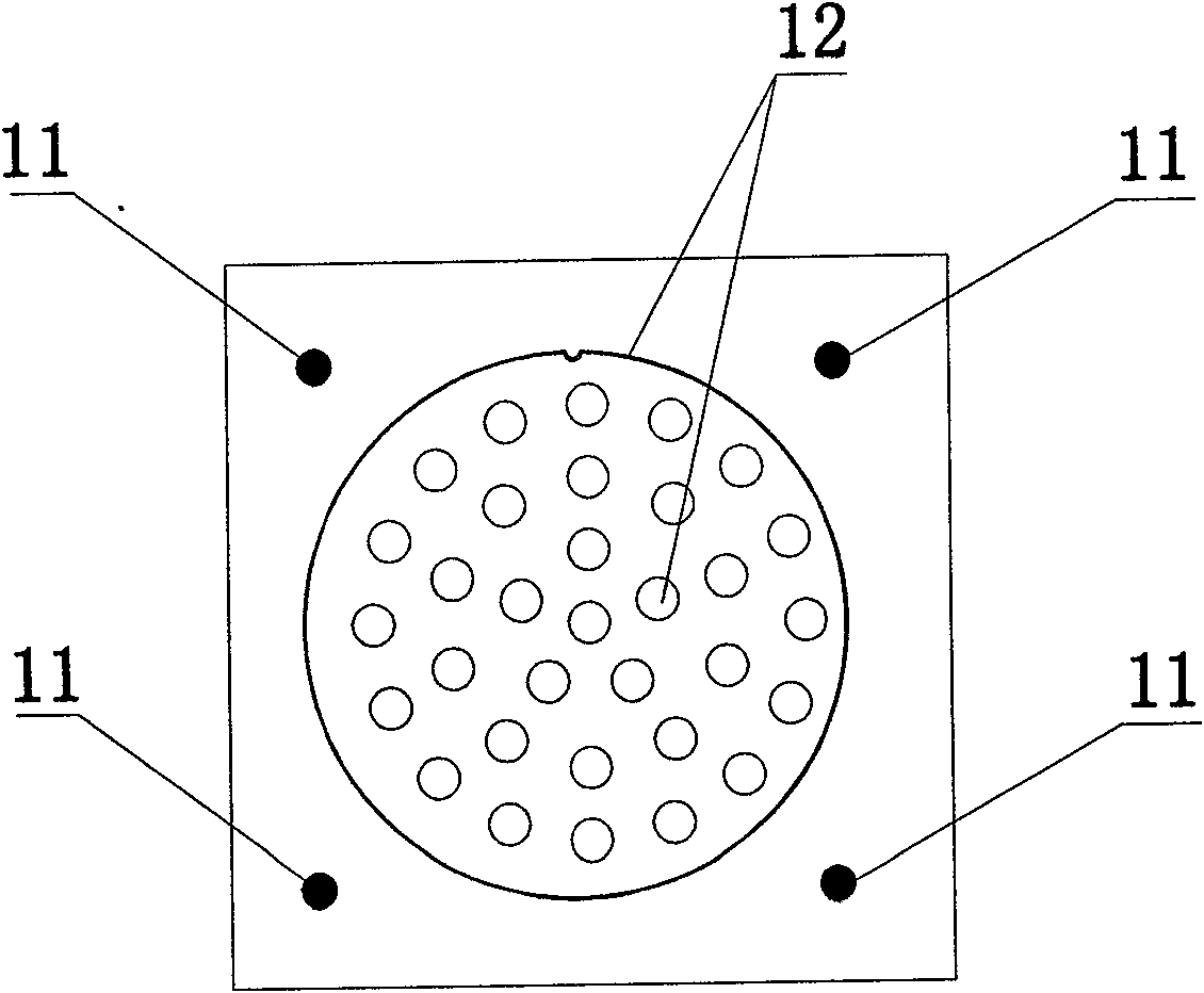
The invention discloses a method for molding a multi-layer plate-type array-structure ceramic filter, relating to a processing and molding method of an electronic element, and comprising the followingmain steps: putting a ceramic body printed with positioning points on a working bench; loading the designed pattern for punching and molding by a computer, and setting parameters for the punching andcutting processes; setting the size of the light energy of a laser light source; controlling a machine vision system to scan the printed pattern on the ceramic body by the computer so as to automatically capture and recognize the positioning points, driving the working bench to move the ceramic body to a cutting position below the laser beam according to the positioning points, controlling a vibrating lens to move according to the position of the positioning points based on the designed pattern for punching and molding by the computer so as to carry out laser punching and cutting, and punching and cutting the inner hole and the outer profile of the ceramic body to mold the ceramic filter. The method for molding a multi-layer plate-type array-structure ceramic filter utilizes the laser toautomatically capture and cut, so that the cutting precision is high, the speed is high, and the damage on the surface of the filter is small. The method for molding a multi-layer plate-type array-structure ceramic filter is applicable to filters with requirements such as small space, high precision, large capacity, ultra-large thickness and diversity, and improves the production efficiency and the qualification rate of the filter products.
Description
technical field [0001] The invention relates to a method for processing and forming electronic components, in particular to a method for forming a ceramic filter with a multilayer plate array structure. Background technique [0002] The multilayer plate array structure ceramic filter molding method, the traditional method adopts the method of die punching, one is that the internal through hole is drilled by a drilling machine, and the outer contour is punched by a die punching machine. The other is to use a mold to punch the inner hole and outer contour at one time with a punch. The disadvantages of the drilling and punching method are: 1. Punching through a punching machine or drilling with a drilling machine, the pressure of the punching machine or drilling machine is high, which will cause cracking and damage to the inner hole and outer contour edge of the ceramic filter after blanking, which will affect the filter. Electrical properties. At the same time, the inner hole...
Claims
Login to View More Application Information
Patent Timeline
 Patent Type & AuthorityApplications(China)
IPC IPC(8): H01P11/00H03H3/00B23K26/38B28D1/14B28D1/22B23K26/382
Inventor童岗杨玲伍虹凌
OwnerCHENGDU HONGMING ELECTRONICS CO LTD