Controlled buckling structures in semiconductor interconnects and nanomembranes for stretchable electronics

A technique for interconnecting structures and stretching components, which is applied to the structure of materials and devices, and the field of stretchable components of devices, which can solve problems such as research limitations

Active Publication Date: 2010-03-24
THE BOARD OF TRUSTEES OF THE UNIV OF ILLINOIS
View PDF6 Cites 67 Cited by
  • Summary
  • Abstract
  • Description
  • Claims
  • Application Information

AI Technical Summary

Problems solved by technology

However, this study was limited by using relatively thin layers (e.g., about 105 nm) of metal films, as the system could have formed electrical conductors that could be stretched by about 10%

Method used


Image

  • Controlled buckling structures in semiconductor interconnects and nanomembranes for stretchable electronics
  • Controlled buckling structures in semiconductor interconnects and nanomembranes for stretchable electronics
  • Controlled buckling structures in semiconductor interconnects and nanomembranes for stretchable electronics

Examples


Embodiment 1

[0186] Example 1: Controlled warp structure in semiconductor nanobelts and its application in stretchable electronic devices

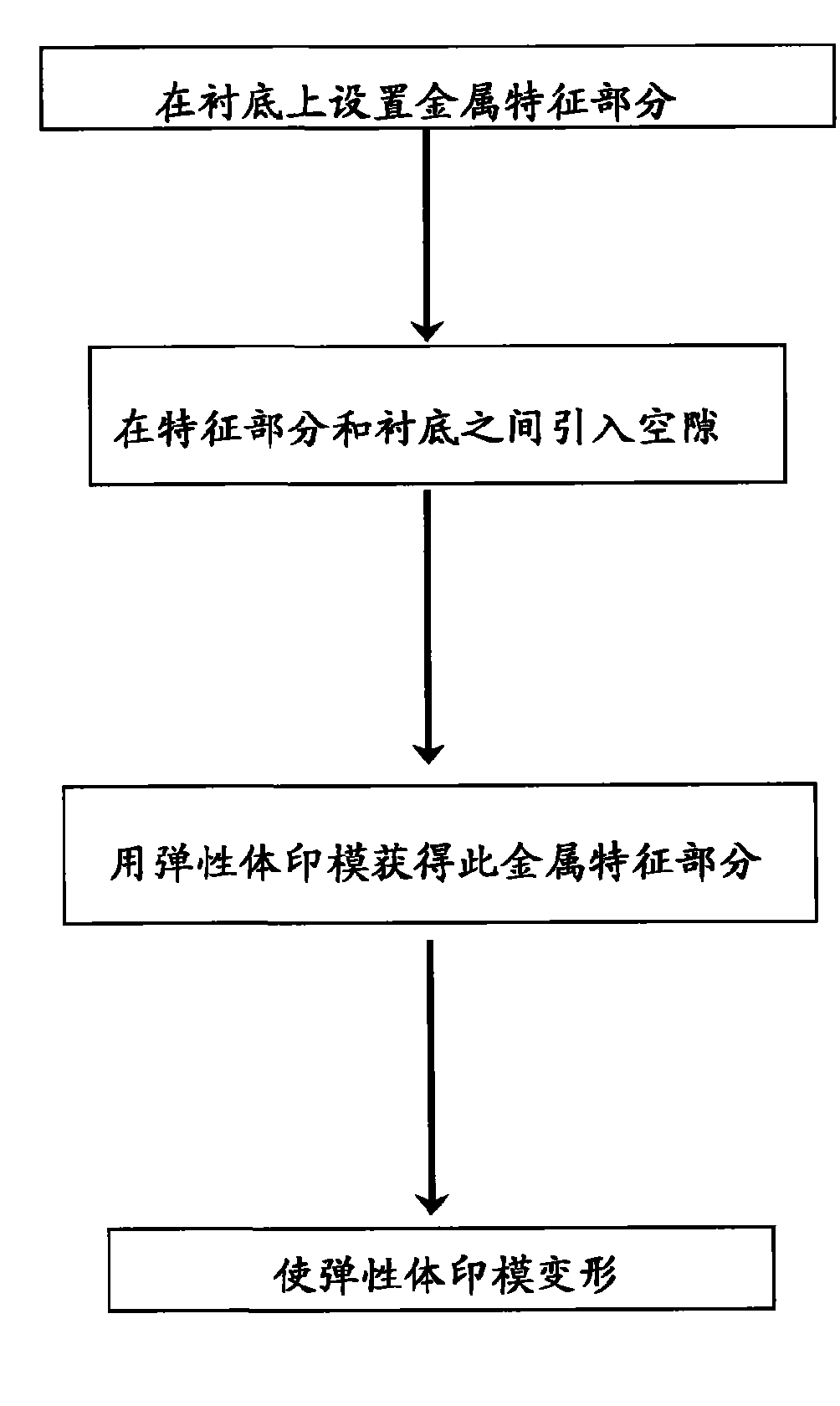
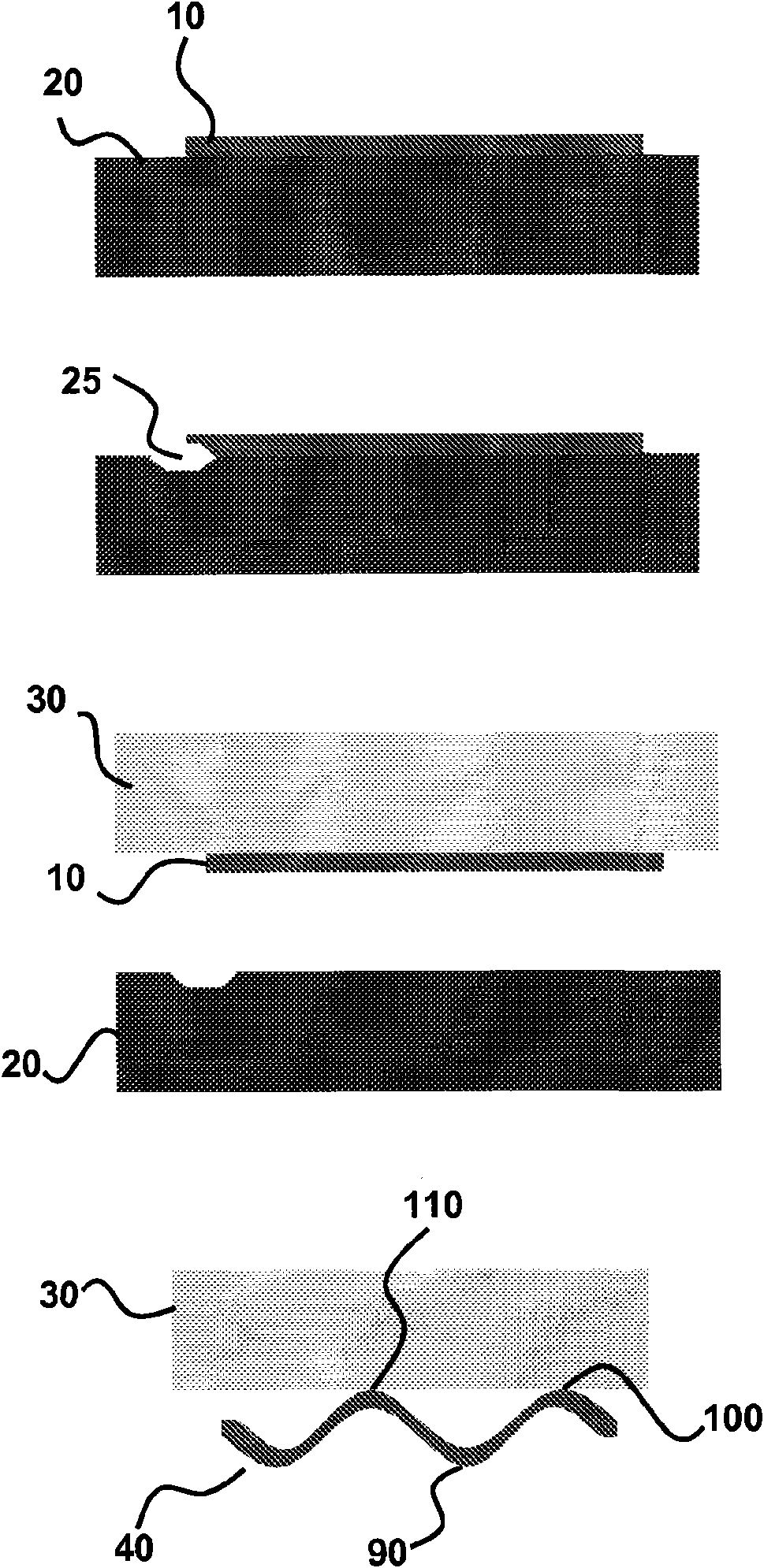
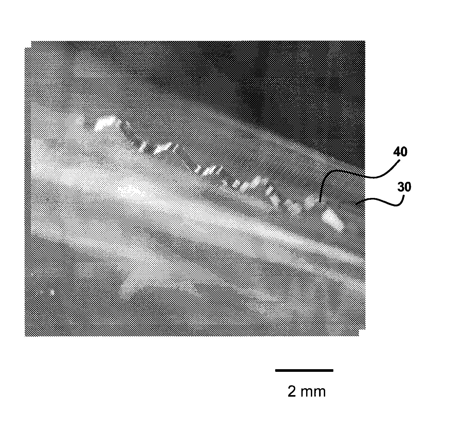
[0187] Important for almost all applications of these materials is the control over the composition, shape, spatial location and / or geometry of the semiconductor nanostructures. While methods exist for defining the material composition, diameter, length, and position of nanowires and nanoribbons, there are relatively few new ways to control their two- and three-dimensional (2D and 3D) structures. Presented here is a mechanistic strategy for creating certain types of 3D shapes that are otherwise difficult to generate in nanoribbons. This embodiment introduces the combined use of lithographically patterned surface chemistry methods to provide spatial control over the adhesive sites and elastic deformation of the support substrate, resulting in well-controlled localized displacement. Precisely designed warp geometries are created in this way in GaAs and ...

Embodiment 2

[0216] Example 2: transfer printing

[0217] Our technical approach uses certain concepts implemented in planar stamp-based printing methods as described previously. While these basic techniques provide an optimistic entry point, many fundamental new capabilities must be introduced to meet the challenges of HARDI (Hemispherical Array Detector Imaging) systems, as described below.

[0218] Figure 32 and 33 A general strategy related to transfer to curved surfaces is shown. The first set of steps ( Figure 32 ) involves the fabrication and manipulation of a thin, spherically curved elastomeric stamp designed to lift interconnected Si CMOS "microchips" off the flat surface of a wafer and then convert that geometry into a hemisphere. Elastomers such as polydimethylsiloxane (PDMS) are obtained by casting and curing liquid prepolymers against high-quality optical elements (i.e., matched convex and concave lenses) selected according to the required radius of curvature to form a ...

Embodiment 3

[0229] Example 3: Biaxially Stretchable "Waved" Silicon Nanofilms

[0230] This example introduces a biaxially stretchable form of single crystal silicon consisting of a two-dimensional warped or "wavy" silicon nanofilm on an elastomeric support. The fabrication process for these structures has been described and various aspects of their geometry in various directions and response to uniaxial and biaxial strain have been revealed. Analytical models of the mechanisms of these systems provide a framework for quantitatively understanding their behavior. These types of materials offer a route to high-performance electronics with fully two-dimensional stretchability.

[0231]Electronic devices exhibiting mechanical bendability are of interest for applications in information displays, X-ray imaging, optoelectronic devices, and other systems. Reversible stretchability is a different but technically challenging mechanical property that will allow devices to achieve functions that ca...


PUM

PropertyMeasurementUnit
thicknessaaaaaaaaaa
thicknessaaaaaaaaaa
thicknessaaaaaaaaaa

Abstract

In an aspect, the present invention provides stretchable, and optionally printable, components such as semiconductors and electronic circuits capable of providing good performance when stretched, compressed, flexed or otherwise deformed, and related methods of making or tuning such stretchable components. Stretchable semiconductors and electronic circuits preferred for some applications are flexible, in addition to being stretchable, and thus are capable of significant elongation, flexing, bending or other deformation along one or more axes. Further, stretchable semiconductors and electronic circuits of the present invention are adapted to a wide range of device configurations to provide fully flexible electronic and optoelectronic devices.

Description

[0001] Cross References to Related Applications [0002] This application claims the benefit of US Provisional Patent Application 60 / 944,626, filed June 18, 2007, and US Provisional Patent Application 60 / 824,683, filed September 6, 2006. Background technique [0003] Since the first demonstration of printed all-polymer transistors in 1994, a great deal of attention has been directed to possible new classes of electronic systems, including flexible integrated electronics on plastic substrates. [Science Vol. 265, pp. 1684-1686, by Garnier F., Hajlaoui R., Yassar A., ​​and Srivastava P.] Recently, a great deal of research has been directed to the development of new solution processable materials for Conductors, dielectrics and semiconducting elements of flexible plastic electronics. Advances in the field of flexible electronics, however, are driven not only by the development of new solution-processable materials, but also by new component geometries, devices, and device assembl...

Claims


Application Information

Patent Timeline
Patent Type & Authority Applications(China)
IPC IPC(8): H01B7/06H01R35/00
CPCH01L31/0203H01L29/1606H01L2924/30105H05K2201/0133H05K1/0283H01L29/7842H05K2201/09045H01L21/6835H01L29/0665H01L27/0688H01L29/7781H01L29/20H01L29/16B82Y10/00H01L21/8221H01L27/0605H01L27/281H05K2203/0271H01L29/78681H01L51/0097B81B3/0078H05K1/0313H01L21/8258H01L27/1446H01L29/78696H01L29/1602H01L29/0673H05K3/20H01L2924/0002H01L27/1292H01L2924/13091H01L2924/00011Y02E10/549Y02P70/50H10K19/201H10K77/111H01L2224/80001H01L2924/00012H01L2924/00H01L21/185H01L21/4857H01L21/76832H01L23/4985H01L23/5387
Inventor J·A·罗杰斯M·梅尔特孙玉刚高興助A·卡尔森W·M·崔M·斯托伊克维奇H·江Y·黄R·G·诺奥李建宰姜晟俊朱正涛E·梅纳德安钟贤H-S·金姜达荣
Owner THE BOARD OF TRUSTEES OF THE UNIV OF ILLINOIS
Why Eureka
Try Eureka