Hybrid fluorescent/phosphorescent oleds

A fluorescent emission and fluorescent host technology, which is applied in semiconductor/solid-state device manufacturing, organic semiconductor devices, semiconductor devices, etc., can solve the problems of limiting the total efficiency of white devices and limited blue light output efficiency, and achieve the effect of improving efficiency.

Active Publication Date: 2010-03-24
乐金显示光电科技(中国)有限公司
View PDF153 Cites 18 Cited by
  • Summary
  • Abstract
  • Description
  • Claims
  • Application Information

AI Technical Summary

Problems solved by technology

[0018] However, all these disclosures show limited blue light output efficiency, which limits the overall efficiency of white devices, because the green and red components of the white emission must be balanced with the blue component in order to obtain ideal CIE coordinates and CRI

Method used


Image

  • Hybrid fluorescent/phosphorescent oleds
  • Hybrid fluorescent/phosphorescent oleds
  • Hybrid fluorescent/phosphorescent oleds

Examples


Embodiment 1-1 to 1-4

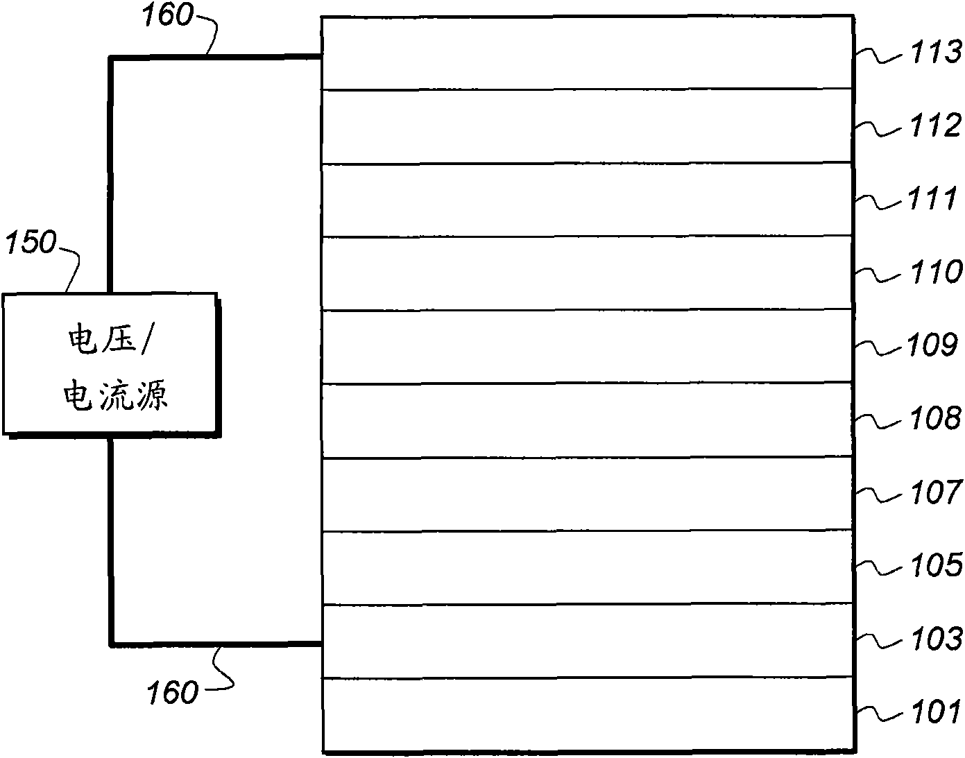
[0482] An EL device (Device 1-1) satisfying the requirements of the present invention was constructed in the following manner:

[0483] 1. A glass substrate coated with an approximately 25 nm layer of indium tin oxide (ITO) as the anode was sequentially sonicated in a commercial detergent, rinsed in deionized water, and exposed to oxygen plasma for approximately 1 minute.

[0484] 2. Next, a hole transport layer of N,N′-di-1-naphthyl-N,N′-diphenyl-4,4′-diaminobiphenyl (host-7 or NPB) was vacuum deposited ( HTL) to a thickness of 75nm.

[0485] 3. Vacuum deposit an exciton / electron blocking layer (EBL) of 4,4',4"-tris(carbazolyl)-triphenylamine (host-6 or TCTA) to a thickness of 10 nm.

[0486] 4. A 5nm light-emitting layer (LEL 1) consisting of a mixture of Host-8 as host and Emitter-1 as blue fluorescent emitter present at a concentration of 1 wt% relative to the host was then vacuum-deposited on the exciton blocking layer.

[0487] 5. A 5 nm thick spacer layer without dope...

Embodiment 2-1 to 2-5

[0498] An EL device (device 2-1) satisfying the requirements of the present invention was constructed in the same manner as devices 1-1 to 1-4, having the following elements: ITO|NPB(75nm)|TCTA(10nm)|Host-8+1% Emitter-1 (5nm) | Host-13 (10nm) | Host-13+8%Ir(ppy) 3 (20nm)|Bphen(25nm)|LiF:Al.

[0499] The device shows a blue fluorescent dopant and a green phosphorescent Ir(ppy) 3 Emission of dopants. at 1mA / cm 2 The luminous efficiency is 39.2cd / A, the CIE (x, y) is (0.232, 0.425), and the external quantum efficiency is 14.2%. Luminous efficiency and EQE are still high at lower current densities. Note that host-13 (spacer and phosphorescent host) has a triplet energy of 2.57 eV compared to host-8 (2.67).

[0500] An EL device not satisfying the requirements of the present invention was constructed in the same manner as 2-1, except that the blue fluorescent emitter was Emitter-2. The concentration was 1% in 2-2, 2% in 2-3, 5% in 2-4, and 7.5% in 2-5. Comparative Example 2-...

Embodiment 3-1

[0504] An EL device (device 3-1) satisfying the requirements of the present invention was constructed in the same manner as devices 1-1 to 1-4, having the following elements: ITO|NPB(75nm)|TCTA(10nm)|Host-22+1% Emitter-1 (5nm) | Host-13 (10nm) | Host-13+8%Ir(ppy) 3 (20nm)|Bphen(20nm)|LiF:Al.

[0505] The device shows a fluorescent dopant from blue and a green (Ir(ppy) 3 ) emission of the phosphorescent dopant. at 1mA / cm 2 , the luminous efficiency is 33.2cd / A, the CIE (x, y) is (0.220, 0.380), and the external quantum efficiency is 13%. Luminous efficiency and EQE are still high at lower current densities. The fluorescent host in the device has a HOMO of -5.59 eV and a triplet energy of 2.76 relative to the fluorescent emitter with a HOMO of -5.69, and the spacer and phosphorescent host with a triplet energy of 2.57.


PUM


Abstract

An electroluminescent device comprises a) a fluorescent light emitting layer comprising a fluorescent emitter and a fluorescent host material wherein the HOMO energy level of the fluorescent host material is not more than 0.1 eV more negative than that of the fluorescent emitter; b) a phosphorescent light emitting layer comprising a phosphorescent emitter and a phosphorescent host material; and c)a spacer layer interposed between the fluorescent light emitting layer and the phosphorescent light emitting layer; wherein the triplet energy of the fluorescent host material is not more than 0.2 eVless than the triplet energy of both the spacer layer material and of the phosphorescent host material. The materials within these layers are selected so that the HOMO and triplet energy levels satisfy certain interrelationships. The invention provides devices that emit light with high luminous efficiency.

Description

technical field [0001] The present invention relates to an organic light emitting diode (OLED) electroluminescent (EL) device comprising a hybrid fluorescent / phosphorescent structure in which the blue fluorescent emitting component is produced with high efficiency while allowing energetically more favorable triplet excitons Diffusion from the blue singlet emitting region to the phosphorescent emitting region provides desirable electroluminescent properties such as high luminescence and energy efficiency. Background technique [0002] Although organic electroluminescent (EL) devices have been known for more than two decades, their performance limitations have hindered many desired applications. In its simplest form, an organic EL device includes an anode for hole injection, a cathode for electron injection, and an organic medium sandwiched between these electrodes to support charge recombination that produces light emission. These devices are also commonly referred to as org...

Claims


Application Information

Patent Timeline
Patent Type & Authority Applications(China)
IPC IPC(8): H01L51/52
CPCH01L2251/5376H01L51/0085H01L51/008H01L51/5044H01L51/5016H01L51/0081H01L51/0079H10K85/321H10K85/322H10K85/324H10K85/342H10K50/131H10K50/11H10K2101/10H10K2101/27
Inventor J·C·迪顿D·Y·康达寇夫M·E·康达可瓦K·P·可路贝D·L·康福
Owner 乐金显示光电科技(中国)有限公司
Why Eureka
Try Eureka