Silicon wafer stage double-stage exchange system by adopting air-floatation planar motor

A technology of plane motor and exchange system, which is applied to electrical components, electromechanical devices, and exposure devices for photoengraving processes, etc., can solve the problems of asymmetric force on the mover, complicated control, high precision of rail docking, etc., so as to avoid high motor power. , The effect of simplifying the control structure and improving the response speed

Active Publication Date: 2010-04-14
TSINGHUA UNIV +1
View PDF8 Cites 38 Cited by
  • Summary
  • Abstract
  • Description
  • Claims
  • Application Information

AI Technical Summary

Problems solved by technology

However, there are also some problems in the double-swap exchange system of the silicon wafer stage. First, the system requires extremely high precision for the docking of the guide rails; Large, which is undoubtedly very important for semiconductor chip factories with high space utilization requirements
The third is that the system needs to use a bridge device with a drive device when exchanging silicon wafers, which increases the complexity of the system
When this stacked drive structure realizes planar motion, both the upper layer linear motor and the silicon wafer stage directly driven by it need to be driven by the bottom layer linear motor, which greatly increases the burden on the bottom layer linear motor, and at the same time

Method used


Image

  • Silicon wafer stage double-stage exchange system by adopting air-floatation planar motor
  • Silicon wafer stage double-stage exchange system by adopting air-floatation planar motor
  • Silicon wafer stage double-stage exchange system by adopting air-floatation planar motor

Examples


Embodiment Construction

[0034] The specific structure, mechanism and working process of the present invention will be further described below in conjunction with the accompanying drawings.

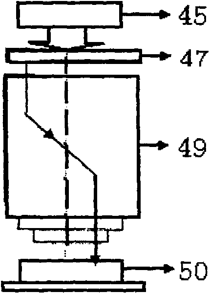
[0035] The basic principle of step and scan projection lithography machine is as follows: figure 1 shown. The deep ultraviolet light from the light source 45 passes through the reticle 47 and the lens system 49 to image a part of the pattern on the reticle on a chip of the silicon wafer 50 . The reticle and the silicon wafer move synchronously in reverse at a certain speed ratio, and finally image all the patterns on the reticle on a specific chip (Chip) of the silicon wafer. The basic function of the wafer motion positioning system (wafer stage) is to carry the wafer during the exposure process and move according to the set speed and direction, so as to realize the precise transfer of the mask pattern to each area on the wafer.

[0036] The traditional step-and-scan projection lithography wafer stage such as ...


PUM


Abstract

The invention relates to a silicon wafer stage double-stage exchange system by adopting an air-floatation planar motor, mainly applied to a photoetching machine system. The silicon wafer stage double-stage exchange system comprises a drill base as well as a silicon wafer stage and a silicon wafer stage driving device having the same structure and respectively working on a preprocessing station and an exposure station. The silicon wafer stage driving device consists of a planar motor and an air-floatation structure, wherein the planar motor adopts a permanent magnetic planar motor, a stepping planar motor, an induction-type planar motor or a switch reluctance planar motor, and consists of a stator and two rotors, wherein the stator is arranged on the top of the drill base, and the rotors are arranged at the bottom of the silicon wafer stage; and the air-floatation structure is formed by a plurality of air-floatation bearings arranged at the bottom of the silicon wafer stage. The system realizes double-stage exchange and stepping scanning motion on the plane by directly driving the silicon wafer stage with the planar motor, thereby improving the productivity, alignment precision and resolution of the photoetching machine.

Description

technical field [0001] The invention relates to a double-swap exchange system for silicon wafer tables of a lithography machine. The system is mainly used in semiconductor lithography machines and belongs to the field of semiconductor manufacturing equipment. Background technique [0002] In the production process of integrated circuit chips, the exposure transfer (photolithography) of the design pattern of the chip on the photoresist on the surface of the silicon wafer is one of the most important processes. The equipment used in this process is called a photolithography machine (exposure machine). The resolution and exposure efficiency of the lithography machine greatly affect the characteristic line width (resolution) and productivity of the integrated circuit chip. As the key system of the lithography machine, the motion accuracy and work efficiency of the silicon wafer ultra-precision motion positioning system (hereinafter referred to as the wafer stage) largely determ...

Claims


Application Information

Patent Timeline
IPC IPC(8): G03F7/20H02K33/18
Inventor 朱煜张鸣汪劲松闵伟尹文生胡金春徐登峰杨开明段广洪田丽许岩
Owner TSINGHUA UNIV
Why Eureka
Try Eureka