Schottky barrier diode and preparation method thereof

A Schottky potential and diode technology, applied in semiconductor/solid-state device manufacturing, electrical components, circuits, etc., can solve the problems of increasing production management complexity, complex process, and high equipment requirements, improving electrical efficiency and reducing potential barriers. Highly effective, simple preparation method

Inactive Publication Date: 2010-04-21
上海芯石微电子有限公司
View PDF2 Cites 11 Cited by
  • Summary
  • Abstract
  • Description
  • Claims
  • Application Information

AI Technical Summary

Problems solved by technology

In order to reduce the forward voltage drop, three methods have been widely used. One is to increase the chip size of the Schottky barrier diode, that is, to increase the area to reduce the forward voltage drop under a given current condition, but this method The cost is greatly increased; the second method is to use metal with low barrier height, but this will increase the leakage current of the device, reduce the reverse voltage and high temperature characteristics, and increase the complexity of production management at the same time; the third is to use silicon The surface of the epitaxial wafer is trenched to increase the contact area. This method is complex in process and requires high equipment

Method used


Image

  • Schottky barrier diode and preparation method thereof
  • Schottky barrier diode and preparation method thereof
  • Schottky barrier diode and preparation method thereof

Examples


Embodiment 1

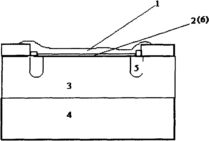
[0032] A thin oxide layer is grown between the silicon epitaxial wafer and the metal, the thickness of the oxide layer is Then sputter or evaporate the metal, and clean the thin oxide layer with a mixed solution of ammonia, hydrogen peroxide and water at a ratio of 1:2:8 at 75°C for 30 minutes, and the alloy forms a silicide as a barrier layer.

[0033] The obtained diode barrier height is 0.629, and the oxide layer thickness is The forward voltage drop is 0.541V.

Embodiment 2

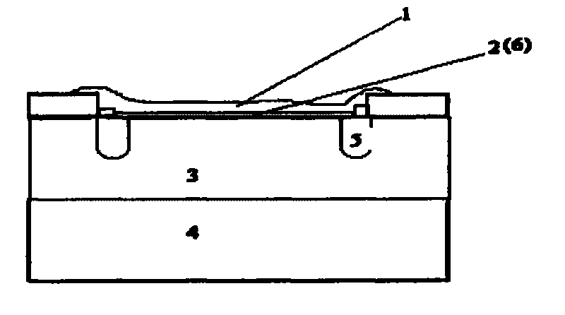
[0035] A thin oxide layer is grown between the silicon epitaxial wafer and the metal, the thickness of the oxide layer is Then sputter or evaporate the metal, and clean the thin oxide layer with a mixed solution of ammonia, hydrogen peroxide and water at a ratio of 1:2:8 at 75°C for 20 minutes, and the alloy forms a silicide as a barrier layer.

[0036] The obtained diode barrier height is 0.624v, and the oxide layer thickness is The forward voltage drop is 0.543V.

Embodiment 3

[0038] A thin oxide layer is grown between the silicon epitaxial wafer and the metal, the thickness of the oxide layer is Then sputter or evaporate the metal, and clean the thin oxide layer with a mixed solution of ammonia, hydrogen peroxide and water at a ratio of 1:2:8 at 75°C for 10 minutes, and the alloy forms a silicide as a barrier layer.

[0039] The barrier height of the obtained diode is 0.655v, and the thickness of the oxide layer is The forward voltage drop is 0.580V. The oxide layer grown in this way is easy to operate, low in cost, and can remove surface particles to improve the yield.


PUM


Abstract

The invention provides a schottky barrier diode and a preparation method thereof. The schottky barrier diode has a structure that an N-type semiconductor is used as a substrate, an N-epitaxial layer is formed on the substrate and a positive electrode is a (blocking layer) metallic material. The preparation method comprises the following steps: cleaning for 10 to 30 minutes with a cleaning reagent of 75 degrees between a silicon epitaxial wafer and a metal to grow a layer of thin oxide layer, wherein the thickness of the oxide layer is between 20 and 100 angstroms; and sputtering or evaporating the metal to ensure that an alloy forms a silicide which servers as a barrier layer so as to form the schottky barrier diode. The preparation method is simple and reduces the barrier height through the participation of the thin oxide layer under the condition with a low cost, the efficient preparation obtains a low forward voltage drop schottky barrier diode, and compared with the conventional diode structure, the schottky barrier diode has a more extensive application range.

Description

technical field [0001] The invention belongs to the technical field of diodes and their preparation, in particular to a Schottky barrier diode and its preparation method. Background technique [0002] Schottky Barrier Diode (SBD) is widely used in DC-DC Converter, Voltage Regulator Module VRM, Telecom / Server, AC Power adapter (Adaptor) and charger (Charger), etc. Instructions attached figure 1 It is a schematic diagram of the structure of a Schottky barrier diode, as shown in the figure, the preparation method of the Schottky barrier diode is to deposit a barrier metal on a silicon epitaxial wafer, or form a metal silicide to form a barrier layer, on which The growth contact metal is used as the lead wire, and the high voltage product generally has a diffusion guard ring. [0003] The invention patent (patent number 02127232.8) applied by Sanyo Electric Co., Ltd. of Japan discloses a manufacturing method of Schottky barrier diodes. InGaP layers are laminated on the surfac...

Claims


Application Information

Patent Timeline
Patent Type & Authority Applications(China)
IPC IPC(8): H01L29/872H01L21/329H01L21/316H01L21/3105
Inventor 杨忠武宋凯霖洪旭峰任宏志
Owner 上海芯石微电子有限公司
Why Eureka
Try Eureka