Erasing and writing method of phase change memory

A technology of phase-change memory and phase-change materials, which is applied in the field of micro-nano electronics, can solve problems such as high cost, and achieve the effects of optimizing cost, reducing device power consumption, and improving thermal efficiency

Active Publication Date: 2010-04-28
SHANGHAI INST OF MICROSYSTEM & INFORMATION TECH CHINESE ACAD OF SCI
View PDF0 Cites 10 Cited by
  • Summary
  • Abstract
  • Description
  • Claims
  • Application Information

AI Technical Summary

Problems solved by technology

However, these methods all need to modify the device itself, and the cost is huge, and by changing the programming method, the read and write operations can save costs, which is the starting point of the present invention

Method used


Image

  • Erasing and writing method of phase change memory
  • Erasing and writing method of phase change memory
  • Erasing and writing method of phase change memory

Examples


Embodiment 1

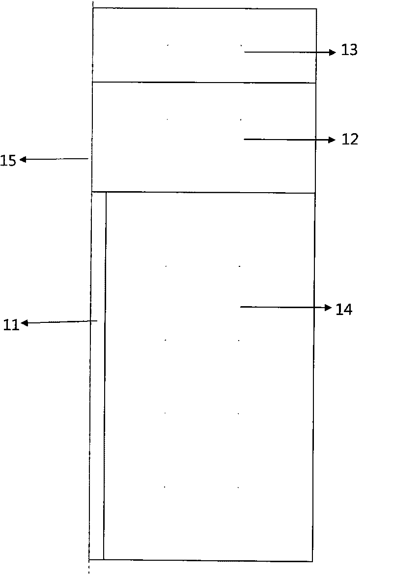
[0062] The axisymmetric structure of the longitudinal section of the phase change memory device is as follows: figure 1 As shown, the material of the lower electrode 11 is W, and the phase change material 12 is Ge 2 Sb 2 Te 5 , the material of the upper electrode 13 is W, and the surrounding insulating material 14 is SiO 2 , the central axis of symmetry 15 . The bottom electrode has a radius of 20 nm. The thickness of the phase change material is 150nm.

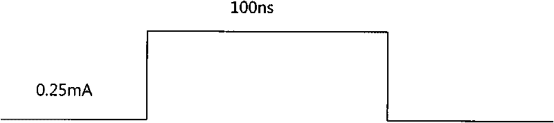
[0063] Step 1, apply a single pulse to the device, such as figure 2 As shown, the pulse height is 0.20-0.30mA, preferably 0.25mA in this embodiment, and the pulse width (operating time) is 20-120ns, preferably 100ns. The device reaches thermal equilibrium at 25-30ns. That is to say, when the device passes current, on the one hand, the phase change material generates heat, and on the other hand, the device dissipates heat through the upper and lower electrodes and the surrounding dielectric materials. When it is less t...

Embodiment 2

[0070] Adopt the same technical solution as in Embodiment 1, except that the pulse signal used is a voltage pulse.

[0071] Step 1, apply a single pulse to the device, such as Figure 9 As shown, the pulse height is 0.3-0.7V, preferably 0.3V in this embodiment, and the pulse width (operating time) is 20-120ns, preferably 100ns. The device reaches thermal equilibrium at 25-30ns. keep the temperature as Figure 11a , 11b shown, where Figure 11b Within the range wrapped by the melting temperature isotherm 111, the phase change material melts, the pulse stops, the temperature drops rapidly, and the melting region forms Figure 11a The amorphous region 112 . The amorphous fails to seal the lower electrode, and fails to form a high-resistance and low-resistance series connection, so the device resistance remains in a low-resistance state. like Figure 14 As shown by the square data points at 141, 142, 143, the resistance has been maintained at 4.3kohm.

[0072] Step 2, appl...


PUM


Abstract

The invention discloses an erasing and writing method of a phase change memory. The erasing operation is realized in a way that: applying a small-pulse-height pulse on a phase change material in the device, wherein the pulse enables the phase change material to right achieve the fusion temperature and partially form amorphous areas in the phase change material; and continuing to applying a plurality of small-pulse-height pulses, and accumulating amorphous areas in the phase change material until the device is transferred from low impedance state to high impedance state. The invention realizes the erasing and writing operations by utilizing the accumulating function; on one hand, low heat produced by the small pulse height is beneficial for stability of the material, and on the other hand, the small pulse height can ensure the application of the phase change memory in the environment requiring low programming current (voltage), thereby reducing the energy consumption of the device and greatly saving the cost for optimizing the device structure under the condition of no change of the device structure of the phase change memory.

Description

technical field [0001] The invention relates to an operation method of a memory, in particular to a method for erasing and writing a phase-change memory that can realize low power consumption. The invention belongs to the technical field of micro-nano electronics. Background technique [0002] Phase change memory technology is based on Ovshinsky's proposal in the late 1960s (Phys. Rev. Lett., 21, 1450-1453, 1968) and early 1970s (Appl. Phys. Lett., 18, 254-257, 1971) The idea that the phase change film can be applied to the phase change storage medium is established, and it is a storage device with low price and stable performance. Phase-change memory can be made on a silicon wafer substrate, and its key materials are recordable phase-change films, heating electrode materials, heat-insulating materials, and lead-out electrode materials. Including how to reduce device material and so on. The basic principle of phase change memory is to use electric pulse signal to act on t...

Claims


Application Information

Patent Timeline
Patent Type & Authority Applications(China)
IPC IPC(8): G11C11/56G11C16/10
Inventor 龚岳峰宋志棠凌云
Owner SHANGHAI INST OF MICROSYSTEM & INFORMATION TECH CHINESE ACAD OF SCI
Why Eureka
Try Eureka