Method for improving Schottky barrier of gallium nitride-based field effect transistor

A GaN-based field and Schottky potential technology, which is applied in semiconductor/solid-state device manufacturing, electrical components, circuits, etc., can solve the problem of large Schottky reverse leakage, parameter drift, and GaN-based field effect transistors. There are no problems such as good stability and reliability, and the effect of improving stability and reliability, reducing reverse leakage, and increasing height

Inactive Publication Date: 2010-05-12
INST OF MICROELECTRONICS CHINESE ACAD OF SCI
View PDF0 Cites 6 Cited by
  • Summary
  • Abstract
  • Description
  • Claims
  • Application Information

AI Technical Summary

Problems solved by technology

However, the existing gallium nitride-based field effect transistors have the problems of large Schottky reverse leakage, and the power performance and breakdown characteristics of the gallium nitride-based field effect transistors are not high.
In addition, GaN-based field-effect transistors have the problem of parameter drift during operation, which leads to poor stability and reliability of GaN-based field-effect transistors

Method used


Image

  • Method for improving Schottky barrier of gallium nitride-based field effect transistor
  • Method for improving Schottky barrier of gallium nitride-based field effect transistor
  • Method for improving Schottky barrier of gallium nitride-based field effect transistor

Examples


Embodiment Construction

[0013] In order to make the objectives, technical solutions and advantages of the present invention clearer, the embodiments of the present invention will be described in further detail below in conjunction with the accompanying drawings.

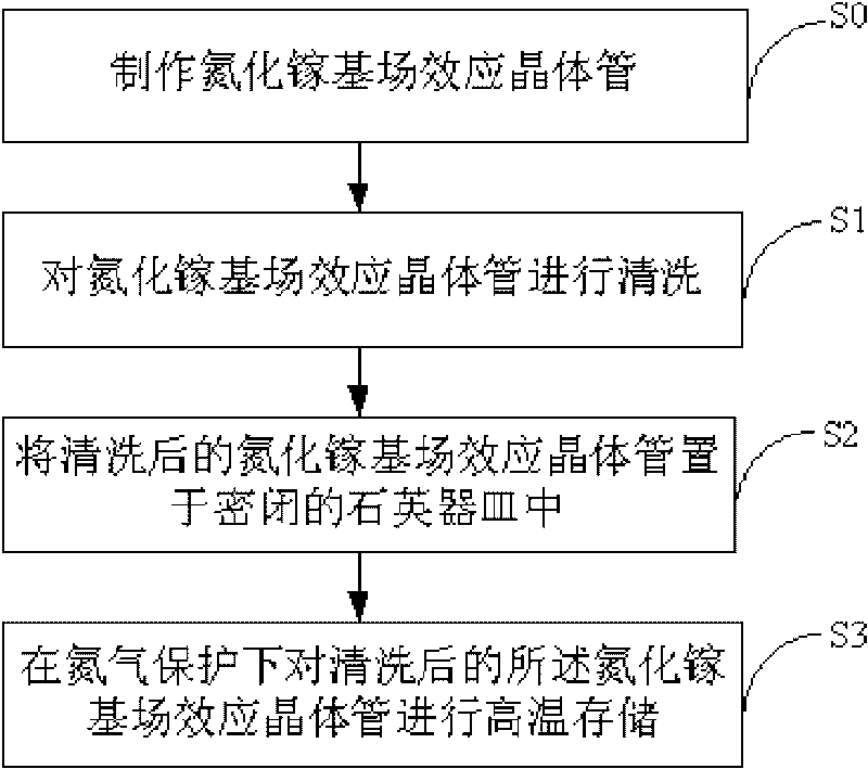
[0014] Such as figure 1 As shown, the embodiment of the present invention provides a method for increasing the Schottky barrier of a gallium nitride-based field effect transistor, including:

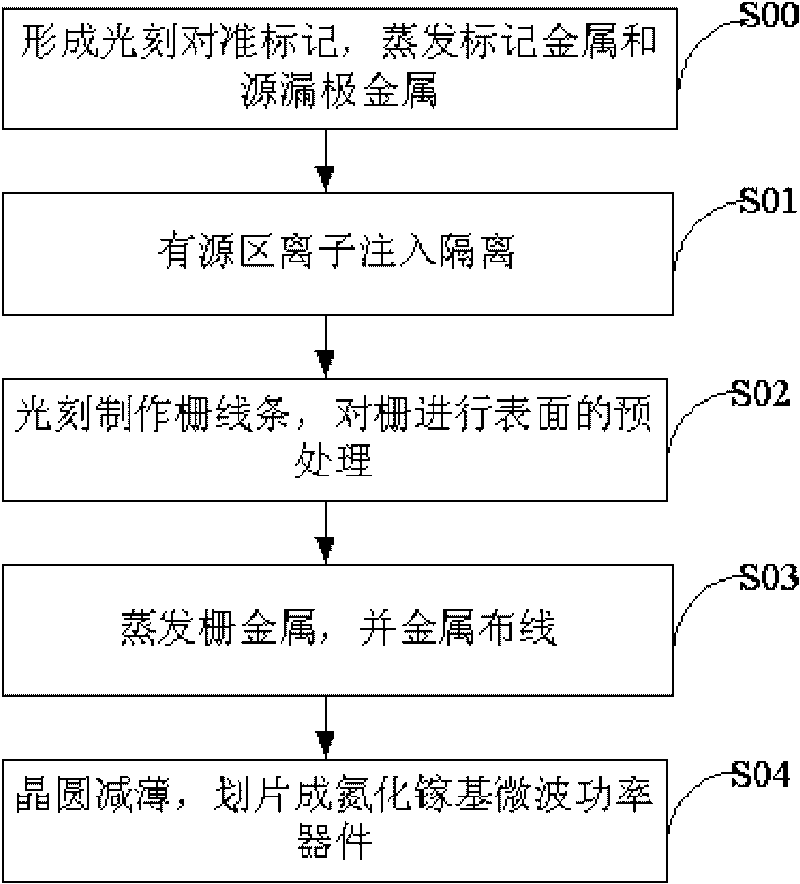
[0015] Step S0, fabricating a gallium nitride based field effect transistor. How to make it in figure 2 Details are described in the illustrated embodiment.

[0016] Step S1: Use acetone and ethanol to clean the GaN-based field effect transistor in sequence.

[0017] Wherein, the cleaning time with acetone is 5 minutes to 10 minutes, the cleaning time with ethanol is 5 minutes to 10 minutes, the processing temperature is room temperature (for example, 25° C.), and the processing container is a closed container.

[0018] Step S2: Put the cleaned GaN-based fiel...


PUM


Abstract

The invention discloses a method for improving a Schottky barrier of a gallium nitride-based field effect transistor, belonging to the technical field of manufacture of semiconductor material device. The method comprises the following steps: cleaning the gallium nitride-based field effect transistor; and storing the cleaned gallium nitride-based field effect transistor under the protection of nitrogen at high temperature. By means of the invention, the height of the Schottky barrier of gallium nitride-based field effect transistor is increased, the reverse leakage f the Schottky barrier of gallium nitride-based field effect transistor is reduced, and the power characteristic and the breakdown characteristic of the gallium nitride-based field effect transistor are improved; therefore, the problem of parameter drift of the gallium nitride-based field effect transistor in the work is solved, and the stability and reliability of the gallium nitride-based field effect transistor are improved.

Description

Technical field [0001] The invention belongs to the field of semiconductor material device manufacturing, and particularly relates to a method for improving the Schottky barrier of a gallium nitride-based field effect transistor. Background technique [0002] In the structure of semiconductor field effect transistors, GaN-based field-effect transistors rely on the gate Schottky barrier to control the channel region. Therefore, the reliability and stability of GaN-based field-effect transistors largely depend on Schottky The reliability and stability of the base gate. The gate leakage current is the main source of low-frequency noise, and the gate reverse breakdown voltage determines the operating voltage and power capacity of the GaN-based field effect transistor. High-quality Schottky contacts are conducive to obtaining high-performance GaN-based field effect transistors. However, the existing GaN-based field effect transistors have the problems of large Schottky reverse leaka...

Claims


Application Information

Patent Timeline
Patent Type & Authority Applications(China)
IPC IPC(8): H01L21/338H01L21/8252
Inventor 赵妙王鑫华刘新宇李诚瞻魏珂郑英奎
Owner INST OF MICROELECTRONICS CHINESE ACAD OF SCI
Why Eureka
Try Eureka