Laser processing method and laser processing apparatus

A laser processing method and laser processing technology, applied in cleaning methods and utensils, laser welding equipment, metal processing equipment, etc., can solve problems such as unfavorable manufacturing speed and quality reduction, and achieve the goal of facilitating manufacturing speed, shortening time, and facilitating high speed effect

Inactive Publication Date: 2010-05-26
DISCO CORP
View PDF11 Cites 13 Cited by
  • Summary
  • Abstract
  • Description
  • Claims
  • Application Information

AI Technical Summary

Problems solved by technology

However, in the case of laser dicing, there is a problem that when the laser beam is irradiated, droplets called debris (debris), which are vaporized components, adhere to the processing surface of the wafer, thereby deteriorating the quality.
Therefore, since the addition of these two processes before and after laser processing is not conducive to improving the manufacturing speed, it is necessary to seek improvement measures.

Method used


Image

  • Laser processing method and laser processing apparatus
  • Laser processing method and laser processing apparatus
  • Laser processing method and laser processing apparatus

Examples


Embodiment Construction

[0027] Hereinafter, an embodiment of the present invention will be described with reference to the drawings.

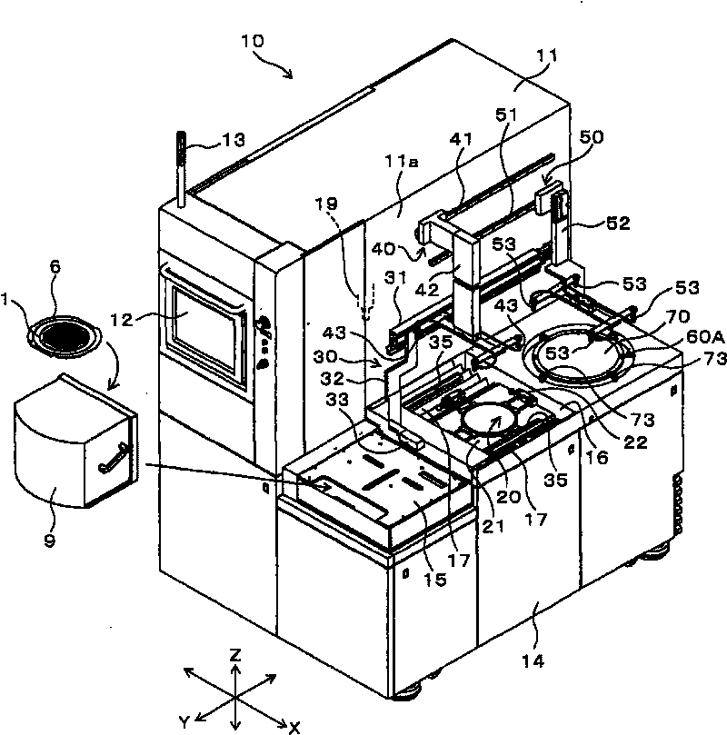
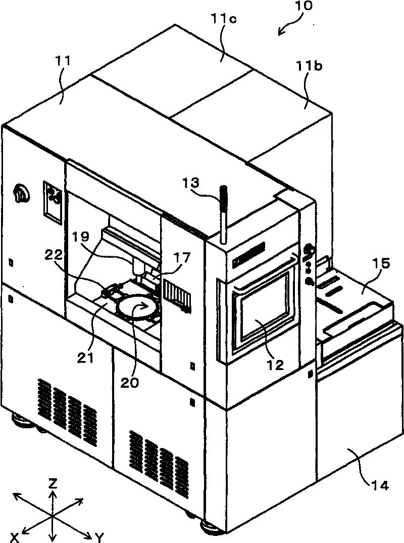
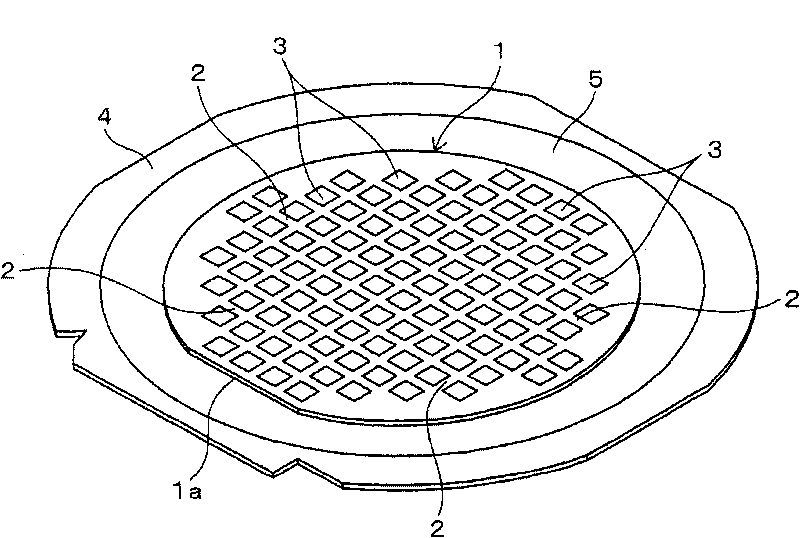
[0028] figure 1 It shows the whole of the laser processing apparatus 10 of one embodiment, figure 2 Indicates the back side. The device 10 is based on image 3 The shown semiconductor wafer (hereinafter, simply referred to as wafer) 1 is a laser cutting device that cuts the wafer 1 by automatic control as a workpiece.

[0029] (1) chip

[0030] use image 3First, the wafer 1 will be described. This wafer 1 is a disk-shaped wafer made of a single crystal material such as silicon. On a part of the outer peripheral portion of the wafer 1, an orientation flat portion (orientation flat) 1a is formed as a mark indicating the orientation of the crystal. . On the surface (processing surface) of the wafer 1, a large number of rectangular chips 3 are divided by dividing lines 2 formed in a grid pattern. On the surface of each chip 3, circuits such as ICs and LSIs (not s...


PUM

PropertyMeasurementUnit
thicknessaaaaaaaaaa

Abstract

The present invention provides a laser processing method and a laser processing apparatus, capable of shortening the time of a protection film forming process of preventing debris caused by laser processing from bringing adverse effect before laser processing and a protection film removing process after laser processing, so as to ensure the quality and further improve manufacturing speed. When the surface of a wafer (1) is coated with water soluble resin (P) to form the protection film (P1) before laser processing, the coated resin (P) is blowed with warm wind to make the resin (P) to be vulcanized rapidly. Furthermore, when the wafer is washed to remove the protection film after laser processing, the cleaning fluid is heated and supplied to the protection film (P1) to accelerate the removing action, and the wafer (1) is blowed with warm wind to be dried rapidly after the protection film (P1) is removed.

Description

technical field [0001] The present invention relates to a laser processing technology for irradiating a workpiece such as a semiconductor wafer with laser light to perform groove processing or cutting processing, and particularly relates to coating a water-soluble resin on the processing surface of the workpiece held on a rotary table, and applying the coated technology for resin removal. Background technique [0002] In the manufacturing process of semiconductor devices, a large number of rectangular chip areas are divided by dividing lines arranged in a grid on the surface of a roughly disc-shaped semiconductor wafer, and ICs (integrated circuits: integrated circuits) are formed in these chip areas. integrated circuits) or LSI (large-scale integration: large-scale integrated circuits), and then, after performing necessary processing such as back grinding on the wafer, the wafer is cut along the planned dividing line to be divided, that is, diced, thereby Each chip region ...

Claims


Application Information

Patent Timeline
Patent Type & Authority Applications(China)
IPC IPC(8): B23K26/00B23K26/18B23K26/42B08B3/10F26B3/06F26B21/00B23K26/38
Inventor 大宫直树
Owner DISCO CORP
Why Eureka
Try Eureka