Method for preparing high-purity semi-insulating silicon carbide crystalloid

A silicon carbide and semi-insulating technology, which is applied in the field of preparing high-purity semi-insulating silicon carbide crystals, can solve problems such as low production efficiency, small crystal point defect concentration, and inability to meet the production needs of silicon carbide crystals, so as to improve resistivity and reduce The effect of microtubule number

Active Publication Date: 2010-06-09
BEIJING TIANKE HEDA SEMICON CO LTD
View PDF0 Cites 26 Cited by
  • Summary
  • Abstract
  • Description
  • Claims
  • Application Information

AI Technical Summary

Problems solved by technology

However, by introducing vanadium as a deep doping level in the crystal, the performance of microwave devices will be affected
In order to eliminate the above effects, the secondary annealing of the crystal is usually introduc

Method used


Image

  • Method for preparing high-purity semi-insulating silicon carbide crystalloid
  • Method for preparing high-purity semi-insulating silicon carbide crystalloid
  • Method for preparing high-purity semi-insulating silicon carbide crystalloid

Examples


Embodiment Construction

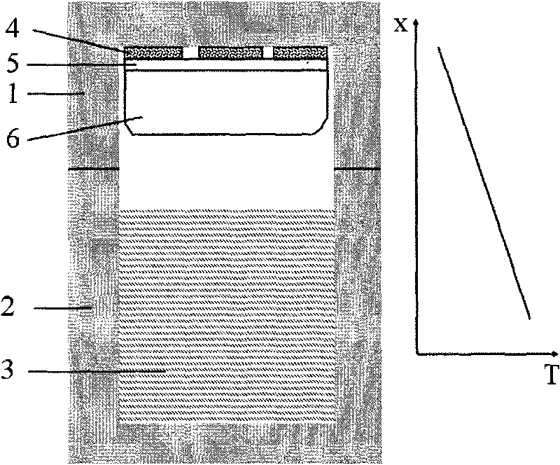
[0020] The present invention is a method for preparing non-doped high-purity semi-insulating silicon carbide crystals. The growth chamber is heated by an induction heating device. The structural diagram of the growth chamber is shown in the attachment figure 1 shown. The growth chamber mainly includes the following parts: graphite cover 1 , graphite crucible 2 , SiC raw material 3 , adhesive 4 , seed crystal 5 , and grown silicon carbide crystal 6 . The seed crystal 5 is bonded to the graphite cover 1 through the adhesive 4, the seed crystal 5 is placed in the upper area of ​​the growth chamber, and the SiC raw material 3 is placed in the lower area of ​​the growth chamber. figure 1 The right side is a schematic diagram of the temperature during the crystal growth process. The abscissa indicates the temperature, and the ordinate indicates the distance from the bottom of the growth chamber. During the growth process, the temperature in the growth chamber gradually decreases alo...


PUM


Abstract

The invention discloses a method for preparing a high-purity semi-insulating silicon carbide crystalloid under the circumstance of compensating elements without deep energy level. The electrical resistivity of the crystalloid is larger than 106 ohm/cm and can reach more than 109 ohm/cm under a proper condition. The electrical resistivity of the crystalloid is controlled by the fast growth speed of the crystalloid, wherein the speed is fast enough to lead the electrical performance of the crystalloid. The requirement of the special growth of the crystalloid is larger than 0.6mm/h, preferably, is more than 2mm/h, and the crystalloid is crystallized and grown under the extreme nonequilibrium state of thermodynamics to increase the concentration of primary point defects such as a hollow bit, a hollow bit group or an inverse bit, and the like, in the crystalloid; the completely grown silicon carbide crystalloid is fast cooled to be 1000-1500 DEG C with faster temperature-reducing speed to ensure the concentration of the point defects of the crystalloid to be thick enough to compensate the different concentration between the shallow donor and the shallow acceptor which are undesignedly doped to achieve the semi-insulating electric performance. The method improves the electrical resistivity of the crystalloid and reduces the quantity of crystalloid microtubules.

Description

technical field [0001] The invention relates to the field of silicon carbide crystal preparation methods, in particular to a method for preparing high-purity semi-insulating silicon carbide crystals. The method grows high-purity semi-insulating silicon carbide crystals without doping deep energy level compensation elements. Background technique [0002] Wide bandgap semiconductor materials represented by silicon carbide (SiC) and gallium nitride (GaN) are the third-generation semiconductors after silicon (Si) and gallium arsenide (GaAs). Compared with Si and GaAs traditional semiconductor materials, SiC has excellent properties such as high thermal conductivity, high breakdown field strength, high saturation electron drift rate and high bonding energy, and has great potential in high temperature, high frequency, high power and radiation resistant devices. Application prospect. Transistors made of semi-insulating silicon carbide are capable of generating power five times the...

Claims


Application Information

Patent Timeline
IPC IPC(8): C30B23/00C30B29/36
Inventor 陈小龙刘春俊王波彭同华鲍慧强王文军王皖燕王刚李龙远
Owner BEIJING TIANKE HEDA SEMICON CO LTD
Why Eureka
Try Eureka