

Plasma display panel and lower substrate thereof
A display panel and plasma technology, applied in the direction of solid cathode parts, cold cathode tubes, etc., can solve the problems that the addressing efficiency and power consumption cannot be improved at the same time, so as to reduce the brightness of the dark field, improve the contrast, reduce the capacitance and ineffective The effect of power consumption
- Summary
- Abstract
- Description
- Claims
- Application Information
AI Technical Summary
Problems solved by technology
Method used
Image

Examples
Embodiment 1
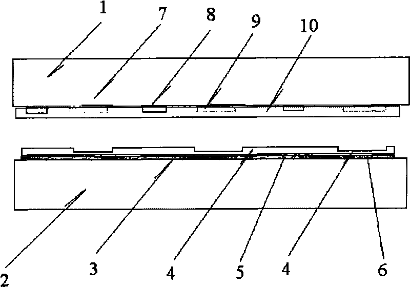
[0013] figure 1 is a schematic structural diagram of a plasma display panel according to an embodiment of the present invention. Such as figure 1 As shown, the plasma display panel includes an upper substrate glass 1 and a lower substrate glass 2 . The upper substrate glass 1 has sustain electrodes (also referred to as X electrodes) 8 and scan electrodes (also referred to as Y electrodes) 9 on the surface of the upper substrate glass 1, and BUS electrodes are formed above the transparent electrodes. Then, the upper substrate glass 1 further includes: a transparent medium 10 with a thickness of about 20 to 40 microns located above the above-mentioned electrodes, so as to protect the electrodes. In addition, the upper substrate glass 1 may further include: a protective medium on the transparent medium 10 , such as a magnesium oxide protective film, so as to avoid particle bombardment. In order to improve the contrast of the display screen, black bars 7 can also be made on the...
Embodiment 2
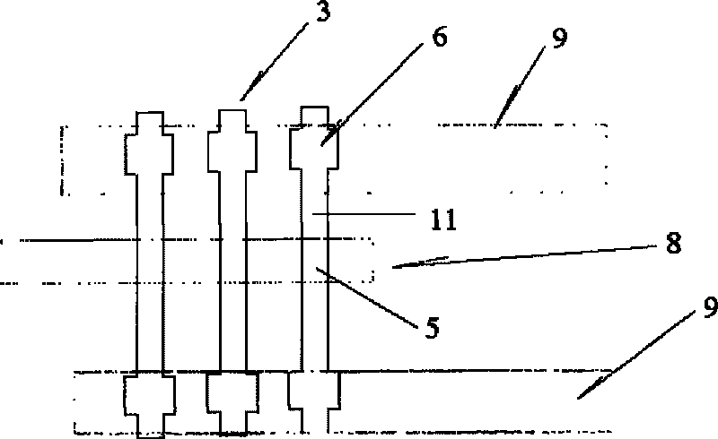
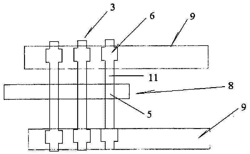
[0021] Such as figure 1 and 2 As shown, the lower substrate of a plasma display panel according to this embodiment includes: figure 2 The address electrode 3 of the structure shown, the address electrode 3 includes: a first part 5 and a second part 6, when connected to the upper substrate, the first part 5 corresponds to the position of the X electrode 8 of the upper substrate, and the second part 6 corresponds to the position of the Y electrode 9 of the upper substrate, wherein the second part 6 is wider than the first part 5 . Since the address electrodes 3 having such a structure are included, the lower substrate according to the present embodiment increases the capacity of the capacitor during the address discharge process and improves the address efficiency. Preferably, the width of the second portion is 1.3 to 1.7 times the width of the first portion.
[0022] Compared with the existing method of overall widening the address electrodes, although the lower substrate a...
Embodiment 3
[0026] A method of fabricating the lower substrate and the plasma display panel in the embodiment of the present invention will be described below.
[0027] In the embodiment of the present invention, by using different thicknesses of dielectric materials and an optimized combination of processes, it is possible to prepare figure 2 addressing electrodes with the structure shown and have as figure 1 The medium of the shown structure, the method mainly adopts the following steps:
[0028] S11, use printing, drying, exposure, development and sintering to complete the fabrication of address electrodes, wherein the width of the address electrodes is appropriately increased under the corresponding Y electrodes, to obtain the following: figure 2 The address electrodes 3 are shown.
[0029] S12 , forming dielectric layers with different thicknesses on the first portion 5 and the second portion 6 of the address electrode 3 . Here, the printing process is used, the first layer is s...
PUM
 Abstract
Description
Claims
Application Information