Room temperature ultrasonic soldering method for area array encapsulated electronic components

An electronic component, ultrasonic technology, applied in the direction of electrical components, electric solid devices, circuits, etc., can solve the problems of residual stress solder joints of welding structures, metallization layers that are easy to inductively heat the surrounding, thermal shock of heat-sensitive materials, etc. Improve reliability and electrical performance, inhibit nucleation and grain growth, eliminate the effects of thermal stress formation

Inactive Publication Date: 2010-06-09
HARBIN INST OF TECH SHENZHEN GRADUATE SCHOOL +1
View PDF0 Cites 10 Cited by
  • Summary
  • Abstract
  • Description
  • Claims
  • Application Information

AI Technical Summary

Problems solved by technology

The first three methods belong to the overall heat conduction heating interconnection method of electronic packaging devices, which will cause residual stress or even micro-cracks in solder joints, and cause thermal shock to heat-sensitive materials, which will bring hidden dangers to the reliability of electronic packaging devices
Laser reflow soldering can achieve local rapid heating to form a reliable interconnection, but the laser can only heat the explicit interconnec

Method used


Image

  • Room temperature ultrasonic soldering method for area array encapsulated electronic components
  • Room temperature ultrasonic soldering method for area array encapsulated electronic components
  • Room temperature ultrasonic soldering method for area array encapsulated electronic components

Examples


Embodiment approach 1

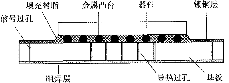
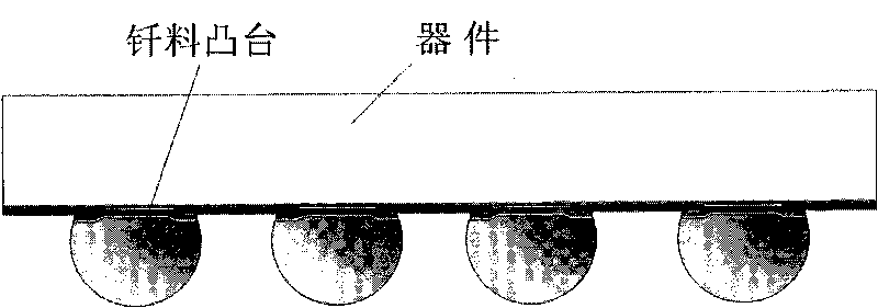
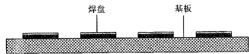
[0027] Embodiment 1: prepare 4×4BGA packaged devices, the diameter of the boss is φ10μm~φ500μm, and the pitch is 10μm~500μm; prepare 4×4BGA corresponding pads, the pad materials are Au / Ni / Cu, and their thicknesses are (10nm~5μm) / (1μm~5μm) / (10μm~100μm); align the interconnection pads of the electronic devices with solder bosses with the pads on the printed circuit board for placement; use a cutting frequency with a fixed frequency of 20~100kHz Weld to a vibration ultrasonic welder. After setting the welding pressure (0.1-6.5bar), welding time (0.1-6s), and input energy (10-900ws), start the ultrasonic welding machine, and the upper sonotrode is pressed tightly on the lower sonotrode under the bonding pressure F driven by the cylinder. On the surface of the upper weldment, the ultrasonic wave is triggered to connect the solder boss and the pad material of the printed circuit board, and finally the upper acoustic pole is retracted, and the process is completed.

Embodiment approach 2

[0028] Embodiment 2: In the second step of Embodiment 1, the Au / Ni / Cu pad is changed to Sn / Cu pad, and its size is (1 μm-10 μm) / (10 μm-100 μm), and the rest of the steps are the same as Embodiment 1 ;

Embodiment approach 3

[0029] Embodiment 3: In the second step of Embodiment 1, the Au / Ni / Cu pad is changed to a Sn-based intermetallic compound layer / Cu pad, and its size is (0.1 μm-10 μm) / (10 μm-100 μm), and the rest The steps are the same as method 1;


PUM

PropertyMeasurementUnit
Thicknessaaaaaaaaaa
Sizeaaaaaaaaaa

Abstract

The invention relates to encapsulation and assembling interconnection methods of micro-electronic and optoelectronic devices, in particular to a room temperature ultrasonic soldering method for area array encapsulated electronic components. The method comprises the following steps of: (1) preparing an area array encapsulated device; (2) preparing a corresponding pad; (3) aligning the area array encapsulated device with the position of the pad; (4) applying certain supersonic vibration and longitudinal pressure on the area array encapsulated device by using a transverse vibration ultrasonic vibrator, so that the solder lug boss generates high-frequency friction with the corresponding pad surface, gradually falls down, and forms metallurgical connection with the pad of the base plate. The invention has the advantages that the tangential vibration ultrasonic waves are utilized at room temperature to connect the area array encapsulated device with the solder alloy solder joint, thereby preventing the soldered structure from undergoing the process of the reheating cycle, eliminating the formation of the heat stress, inhibiting the nucleation and grain growth of the intermetallic compounds and enhancing the reliability and the electrical performance of the joints. The method also has the advantages of simple procedure, high speed, no soldering flux, no need of strict surface cleaning, and the like.

Description

technical field [0001] The invention relates to a packaging, assembly and interconnection method for microelectronic and optoelectronic devices, in particular to a room temperature ultrasonic soldering method for surface array packaged electronic components. Background technique [0002] With the development of electronic packaging devices in the direction of high density, area array packaging technologies such as ball grid array packaging (BGA: BallGrid Assembly), chip scale packaging (CSP: Chip Scale Packaging), and chip multilayer three-dimensional packaging have emerged. Area array packaging technology is a method in which chips are directly mounted and interconnected with a substrate in a boss array structure. The packaging and interconnection structure is as follows: figure 1 shown. The flip-chip soldering process can be further divided into reflow soldering, thermocompression, thermosonic soldering and conductive adhesive interconnection. When using conductive adhes...

Claims


Application Information

Patent Timeline
IPC IPC(8): H01L21/607
CPCH01L24/81H01L2224/73204H01L2224/16225H01L2224/32225H01L2924/351
Inventor 李明雨王晓林计红军汉晶区大公张志能
Owner HARBIN INST OF TECH SHENZHEN GRADUATE SCHOOL
Why Eureka
Try Eureka