

BiFeO3 film resistor memory structure and preparation method thereof
A thin film resistor and memory technology, applied in electrical components and other directions, to achieve the effects of good density, easy control of chemical composition, and simple operation
- Summary
- Abstract
- Description
- Claims
- Application Information
AI Technical Summary
Problems solved by technology
Method used
Image

Examples
Embodiment 1
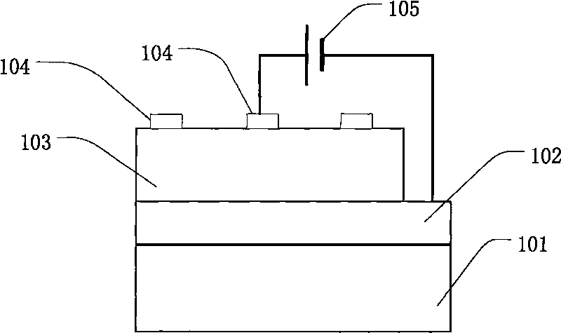
[0028] Embodiment 1 prepares BiFeO 3 memory device
[0029] (1) Preparation of BiFeO 3 Sol: Fully mix diethanolamine with a small amount of ethylene glycol methyl ether, heat to boiling, and cool naturally to obtain mixed solution A; Fe(NO 3 ) 3 .5H 2 After O was dissolved in ethylene glycol methyl ether at room temperature, Bi(NO 3 ) 3 .9H 2 O, heated to 80 ° C for 1 h, cooled to room temperature, and mixed liquid B was obtained. At room temperature, drop the mixed solution A into the mixed solution B, adjust the concentration to 0.2mol / L, stir well for 2-4h, filter, and cool to obtain the precursor solution.
[0030] (2) Preparation of BiFeO 3 Thin film: BiFeO 3 Precursor in LaNiO 3 On the covered Si substrate, the thin film was prepared by spin coating method, and the number of layers was six. Adjust the glue-spinning parameters and time, and pretreat each layer of wet film on a hot plate. The glue-spinning parameter can be 3000 rpm, the time is 30 seconds, and ...
Embodiment 2
[0034] (1) BiFeO 3 The preparation of thin films and devices is the same as (1) and (2) of Example 1.
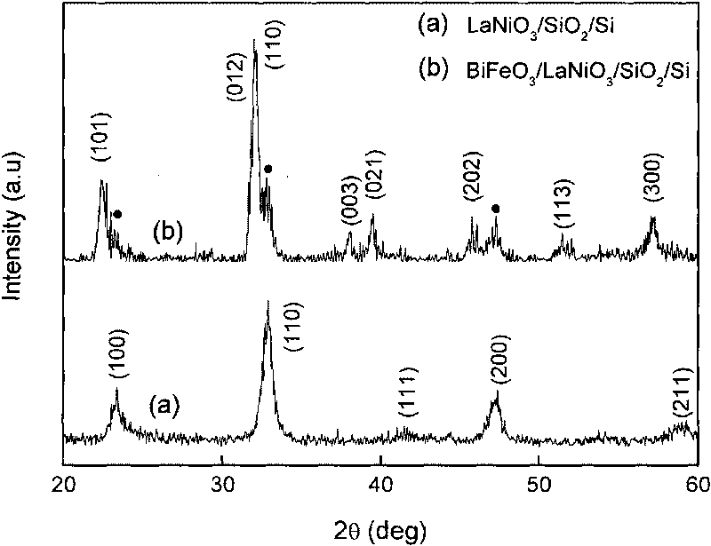
[0035] (2) The above BiFeO 3 The film is heat-treated at 500°C for 30 minutes at a constant temperature. In this way, well-crystallized and dense BiFeO can be obtained 3 thin film, and the absence of Bi 2 Fe 4 o 9 and other miscellaneous phases.
[0036] (3) BiFeO 3 The making of surface electrode is the same as step (4) of embodiment 1.
Embodiment 3
[0038] (1) BiFeO 3 The configuration of the solution is the same as the step (1) of Example 1.
[0039] (2) Preparation of BiFeO 3 Thin film: BiFeO 3 Precursor in clean Pt / TiO 2 / SiO 2 / Si substrate, prepare thin film by spin coating method, the number of layers is six. Adjust the glue-spinning parameters and time, and pretreat each layer of wet film on a hot plate. The glue-spinning parameter is 3000 rpm, the time is 30 seconds, and the pretreatment temperature of each layer is 350° C., and the time is 5 minutes. Repeat the glue-spinning-pretreatment-re-spinning process to get a certain thickness of BiFeO 3 Thin film (200-300nm). .
[0040] (3) BiFeO 3 The heat treatment of the film and the fabrication of the upper surface electrodes are the same as the steps (3) and (4) of Example 1.
PUM
| Property | Measurement | Unit |
|---|---|---|
| Diameter | aaaaa | aaaaa |
Abstract
Description
Claims
Application Information