

Preparation method of holographic grating photoresist patterns with multiple shapes and narrow line widths of hundreds of nanometers
A holographic grating and photoresist technology, which is applied in microlithography exposure equipment, photoengraving process of pattern surface, diffraction grating, etc. effect of duration
- Summary
- Abstract
- Description
- Claims
- Application Information
AI Technical Summary
Problems solved by technology
Method used
Image

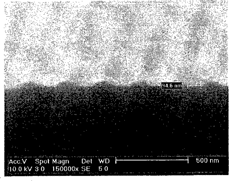
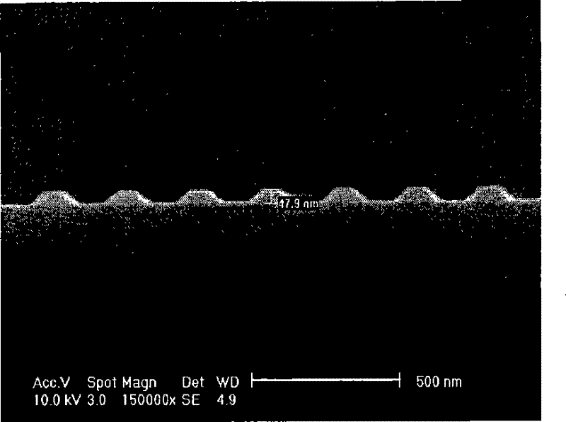
Examples
Embodiment Construction
[0040] In order to make the object, technical solution and advantages of the present invention clearer, the present invention will be described in further detail below in conjunction with specific embodiments and with reference to the accompanying drawings.
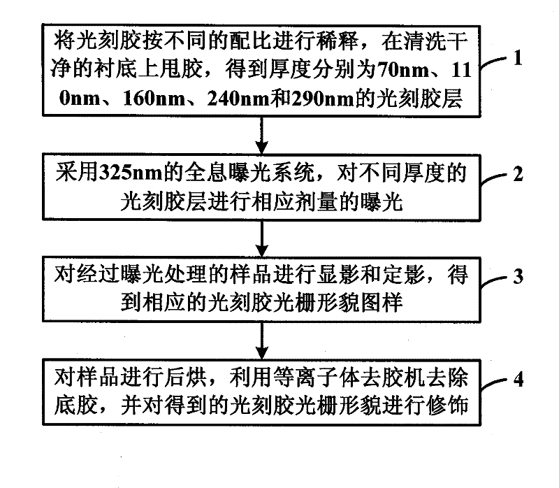
[0041] Such as figure 1 as shown, figure 1 It is a flow chart of a method for preparing a holographic grating photoresist pattern with a narrow line width of a hundred nanometers and various shapes provided by the present invention, and the method includes:
[0042] Step 1: Dilute the photoresist according to different proportions, and shake the glue on the cleaned substrate to obtain photoresist layers with thicknesses of 70nm, 110nm, 160nm, 240nm and 290nm;
[0043] Step 2: Use a 325nm holographic exposure system to expose photoresist layers with different thicknesses in corresponding doses;
[0044] Step 3: developing and fixing the exposed sample to obtain the corresponding photoresist grating pattern;
[0045] Ste...
PUM
| Property | Measurement | Unit |
|---|---|---|
| thickness | aaaaa | aaaaa |
| thickness | aaaaa | aaaaa |
Abstract
Description
Claims
Application Information