TFT-LCD (thin film transistor-liquid crystal display) array substrate and manufacture method thereof

An array substrate and substrate technology, applied in the field of thin film transistor liquid crystal display structure and its manufacture, can solve the problems of low aperture ratio and small storage capacitance

Active Publication Date: 2010-06-16
K TRONICS (SUZHOU) TECH CO LTD +1
View PDF0 Cites 38 Cited by
  • Summary
  • Abstract
  • Description
  • Claims
  • Application Information

AI Technical Summary

Problems solved by technology

[0005] The purpose of the present invention is to provide a TFT-LCD array substrate and its manufacturing method, which can effect

Method used


Image

  • TFT-LCD (thin film transistor-liquid crystal display) array substrate and manufacture method thereof
  • TFT-LCD (thin film transistor-liquid crystal display) array substrate and manufacture method thereof
  • TFT-LCD (thin film transistor-liquid crystal display) array substrate and manufacture method thereof

Examples


Embodiment approach

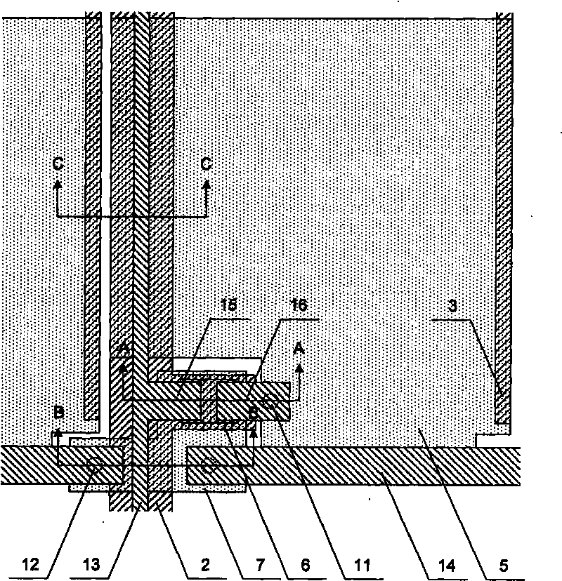
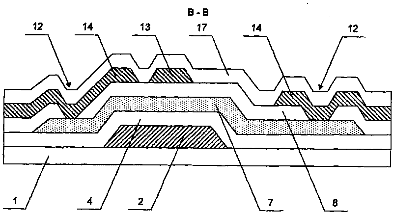
[0069] The five-time patterning process described above is only an implementation method of the TFT-LCD array substrate manufacturing method of the present invention. Under the guiding idea of ​​placing the common electrode line under the data line, it can also be added or reduced in actual use. The number of processes or other processes are used to form the array substrate.

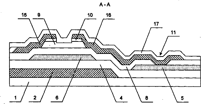
[0070] Figure 26 It is a flow chart of a method for forming an active layer, a first contact via hole and a second contact via pattern in the manufacturing method of the TFT-LCD array substrate of the present invention. exist Figure 25 In the technical solution shown, step 3 specifically includes:

[0071] Step 311, sequentially depositing a gate insulating layer, a semiconductor layer and a doped semiconductor layer on the substrate after step 2;

[0072] Step 312, coating a layer of photoresist;

[0073]Step 313, using a two-tone mask to expose the photoresist, so that the photoresist forms a pho...


PUM


Abstract

The invention relates to a TFT-LCD (thin film transistor-liquid crystal display) array substrate and a manufacture method thereof. The TFT-LCD array substrate comprises a grid line formed on the substrate, a data line and a public electrode line, wherein a pixel electrode forms in a pixel region limited by the grid line and the data line, and a thin film transistor forms on the cross place of the pixel region; and the public electrode line is parallel to the data line and positioned below the data line. Through placing the public electrode line below the data line, the invention maximally reduces an area occupied by the public electrode line in the pixel region and enhances pixel opening ratio on one hand, and can play a shading role on the other hand. Meanwhile, because only one first passivation layer exists between the public electrode line and the pixel line, the distance between two poles of a storage capacitance is greatly reduced and the storage capacitance is enhanced.

Description

technical field [0001] The invention relates to a thin film transistor liquid crystal display structure and a manufacturing method thereof, in particular to a TFT-LCD array substrate and a manufacturing method thereof. Background technique [0002] In the flat panel display technology, due to the thin film transistor liquid crystal display (Thin Film TransistorLiquid Crystal Display, referred to as TFT-LCD) has the characteristics of low power consumption, relatively low manufacturing cost and no radiation, so TFT-LCD occupies a dominant position in the flat panel display market. leading position. Generally, a TFT-LCD is formed by combining an array substrate and a color filter substrate. [0003] At present, the prior art TFT-LCD array substrate usually adopts the bottom gate structure etched in the back channel. The main structure includes a set of gate lines and a set of data lines perpendicular to the gate lines. The adjacent gate lines and data lines define the pixels....

Claims


Application Information

Patent Timeline
IPC IPC(8): G02F1/1362H01L27/12H01L21/84G03F7/00
CPCH01L27/1255H01L27/124
Inventor 张弥
Owner K TRONICS (SUZHOU) TECH CO LTD
Why Eureka
Try Eureka