Preparation method of Cu/Ta nanometer multilayer film with crystal particle dimension difference

A grain size, nano-multilayer technology, applied in coating, metal material coating process, ion implantation plating, etc., can solve the problems of low ductility and undiscovered problems, achieve low cost, improve mechanical properties, and highly operable effect

Inactive Publication Date: 2010-06-23
山东铭特金属材料科技有限公司
View PDF0 Cites 8 Cited by
  • Summary
  • Abstract
  • Description
  • Claims
  • Application Information

AI Technical Summary

Problems solved by technology

Since the 1990s, people began to discover in the process of continuously pursuing the optimization of the mechanical properties of nano-film materials that nano-sized metal multilayer films have superhard effects and supermodulus effects, which impr

Method used


Image

  • Preparation method of Cu/Ta nanometer multilayer film with crystal particle dimension difference
  • Preparation method of Cu/Ta nanometer multilayer film with crystal particle dimension difference
  • Preparation method of Cu/Ta nanometer multilayer film with crystal particle dimension difference

Examples


preparation example Construction

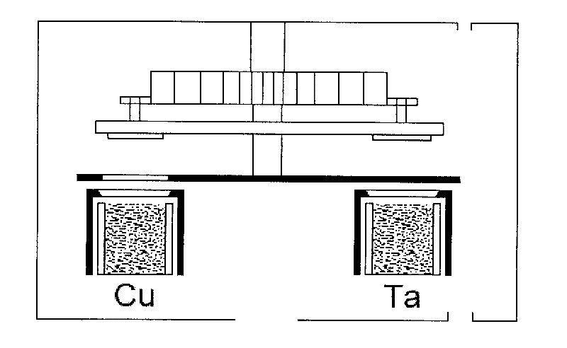
[0025] The preparation process of the Cu / Ta nanometer multilayer film, wherein the DC magnetron sputtering current of the Cu target during double target sputtering is 0.1-0.15A, and the voltage is 200V; the Ta DC magnetron sputtering current is 0.15-0.2 A, the voltage is 250V; the negative bias is 100V, and the distance between the substrate and the target is 5-8cm.

[0026] The ambient temperature of the substrate during deposition is room temperature, about 290-300K.

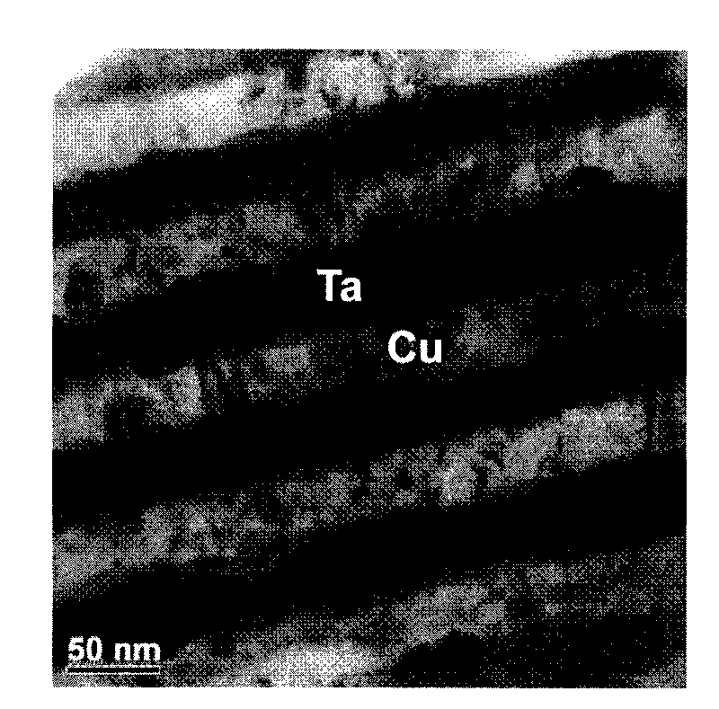
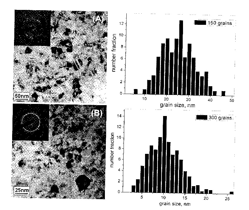
[0027] The present invention adds an important technical step in the process of synthesizing the multilayer film: adopting different sputtering powers to the Cu target and the Ta target, so that the metal nano multilayer film obtains different grain sizes, see figure 2 . The alternating structure of coarse-grained material and fine-grained material improves the strength and plastic deformation ability of the metal nano-multilayer film.

example 1

[0029] The specific technological parameter of the manufacture method of Cu / Ta nanometer multilayer film of the present invention is: adjust the Cu target DC magnetron sputtering current to be 0.15A, the Cu target DC magnetron sputtering power is 30W, and the deposition time is 83 seconds; The Ta target DC magnetron sputtering current is 0.2A, the Ta target DC magnetron sputtering power is 50W, and the deposition time is 143 seconds. The substrate temperature is room temperature. The thus obtained Cu / Ta nanometer multilayer film has a modulation wavelength of 70 nanometers. Wherein the Cu layer is 35 nanometers, and the Ta layer is also 35 nanometers.

example 2

[0031] The concrete process parameter of the manufacture method of Cu / Ta nanometer multilayer film of the present invention is: adjust the Cu target DC magnetron sputtering current to be 0.15A, the Cu target DC magnetron sputtering power is 30W, and the deposition time is 60 seconds; The Ta target DC magnetron sputtering current is 0.2A, the Ta target DC magnetron sputtering power is 50W, and the deposition time is 102 seconds. The substrate temperature is room temperature. The thus obtained Cu / Ta nanometer multilayer film has a modulation wavelength of 50 nanometers. Wherein the Cu layer is 25 nanometers, and the Ta layer is also 25 nanometers.


PUM

PropertyMeasurementUnit
Hardness valueaaaaaaaaaa

Abstract

The invention discloses a method for preparing a metal nanometer multilayer film with different crystal particle dimension by adopting magnetic control sputtering technology; the Cu/Ta nanometer multilayer film is alternately composed of a Cu layer and a Ta layer, and the ratio of the thickness of two layers is 1:1, the modulated wave length is 5-140nm, and the total thickness is 1mum; wherein the size of the Cu layer crystal particle dimension is equivalent to the thickness of the film layer, and the size of the Ta layer crystal particle dimension is 1/4 of the thickness of the film, and the Cu layer and the Ta layer have obvious crystal particle dimension difference; the hardness of the Cu/Ta nanometer multilayer film is increased by 35 percent compared by the traditional multilayer film material, the stretching extensibility exceeds 5 percent and is far more than that of the traditional multilayer film material. The hardness and the plasticity of the Cu/Ta nanometer multilayer film are optimized on the mechanical property; the metal nanometer multilayer film with different crystal particle dimension can be widely applied to very-large-scale integration circuit devices, protective coatings and functional coatings of various precise instruments and the like.

Description

technical field [0001] The invention relates to a method for preparing a metal thin film, more specifically to a method for preparing a Cu / Ta nanometer multilayer film with grain size differences. Background technique [0002] The strength of nano-film materials is usually 3-10 times that of similar coarse-grained materials, indicating that they have excellent mechanical properties and have been widely used in industrial production, such as ultra-large-scale integrated circuit devices with increasing densification, Protective and functional coatings for various precision instruments. However, the plastic deformation effect of nano-film materials is far less than that of coarse-grained materials. As the grain size decreases, the plastic-ductile deformation of materials also decreases, making materials more prone to failure behavior. For example, Baracaldo's research on steel nanomaterials containing 0.55% carbon found that the elongation rate of the grain size was 900nm exce...

Claims


Application Information

Patent Timeline
IPC IPC(8): C23C14/35C23C14/14
Inventor 黄平许明王飞徐可为
Owner 山东铭特金属材料科技有限公司
Why Eureka
Try Eureka