Laser scanning scattering detection and classification system for silicon slice surface defects

A technology of silicon wafer surface, laser scanning, applied in scattering characteristic measurement, optical test defect/defect, optics, etc., can solve the problem of production line yield decline, etc., to achieve the effect of improving working voltage, good reliability and improving sensitivity

Inactive Publication Date: 2010-06-30
上海傲世控制科技股份有限公司
View PDF0 Cites 17 Cited by
  • Summary
  • Abstract
  • Description
  • Claims
  • Application Information

AI Technical Summary

Problems solved by technology

If such problems cannot be detected and resolved in time,

Method used


Image

  • Laser scanning scattering detection and classification system for silicon slice surface defects
  • Laser scanning scattering detection and classification system for silicon slice surface defects

Examples


Example Embodiment

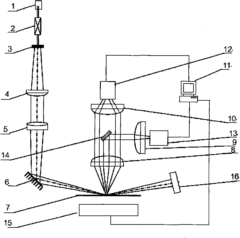
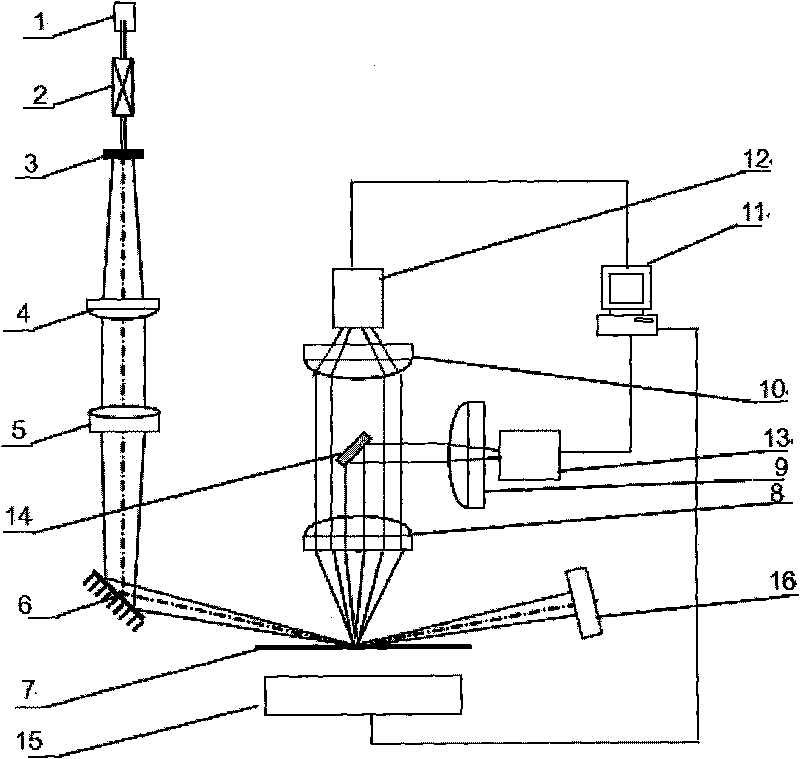
[0017] The preferred embodiments of the present invention are given below in conjunction with the accompanying drawings to illustrate the technical solutions of the present invention in detail. Such as figure 1 The schematic diagram of the principle of the laser scanning scattering detection and classification system for the surface defects of the silicon wafer is also a schematic diagram of the structure of the best embodiment of the present invention. As can be seen from the figure, the structure of the system includes: the light beam emitted by the laser light source assembly 1 advances In the direction of the Faraday isolator 2, the double-concave lens 3 and the first plano-convex lens 4, the beam expander system, the double cemented focusing lens 5, the beam is deflected by the plane mirror 6 and obliquely focused and incident on the surface of the measured silicon wafer 7 , The silicon wafer 7 is located on the worktable 15; the scattered light on the surface of the silic...


PUM

PropertyMeasurementUnit
Caliberaaaaaaaaaa

Abstract

The invention discloses a laser scanning scattering detection and classification system for silicon slice surface defects. A silicon slice to be detected is placed on a high-stability silicon slice workbench, a bunch of focused laser is adopted to irradiate the surface plane of the silicon slice to be detected from an inclined direction, and scattered lights generated by defects are collected through round narrow channel collection and circular wide channel collection by two pairs of plano-convex lenses along the direction close to the normal line of the silicon slice surface and the direction proximately parallel to the silicon slice surface, thus being detected by two photoelectric detectors. Bi-channel photoelectric signal strength and relative ratio thereof are respectively detected by the two photoelectric detectors, and classification detection on defects in tens of nanometers on the silicon slice surface can be carried out by comparing the bi-channel photoelectric signal strength and the relative ratio thereof with a preset threshold value.

Description

technical field [0001] The invention relates to a laser scanning scattering detection and classification system, in particular to a laser scanning scattering detection and classification of silicon chip surface defects with simple structure, high sensitivity, fast detection speed, and the ability to classify and locate silicon chip surface defects system. Background technique [0002] Every step of chip production can introduce defects and contamination either mechanically or artificially. In recent years, due to the continuous increase of silicon chip size and the sharp reduction of integrated circuit graphic feature size, the chip structure has become more complex, and the impact of defect density on yield has become more and more prominent. If such problems cannot be discovered and resolved in time, the yield of the production line will drop significantly. [0003] Laser scanning scattering detection technology for silicon wafer surface defects has been developed rapidl...

Claims


Application Information

Patent Timeline
IPC IPC(8): G01N21/88G01N21/49G02B17/08G02B5/08
Inventor 王毅强陈建芳程兆谷许永锋敖计祥黄惠杰
Owner 上海傲世控制科技股份有限公司
Why Eureka
Try Eureka