Method for pretreating technical cavity of plasma device

A process chamber and pretreatment technology, which is applied in the direction of metal material coating process, gaseous chemical plating, coating, etc., can solve the problem of poor bonding force between the protective layer and the inner wall of the process chamber, so as to reduce the generation of particle pollutants, High adhesion performance and enhanced corrosion resistance

Active Publication Date: 2010-06-30
BEIJING NAURA MICROELECTRONICS EQUIP CO LTD
View PDF0 Cites 11 Cited by
  • Summary
  • Abstract
  • Description
  • Claims
  • Application Information

AI Technical Summary

Problems solved by technology

[0007] The invention provides a method for pretreatment of a plasma device process chamber to solve the problem of poor bonding between the protective layer formed by the existing method and the inner wall of the process chamber

Method used


Image

  • Method for pretreating technical cavity of plasma device
  • Method for pretreating technical cavity of plasma device

Examples


Embodiment 1

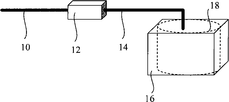
[0046] In this embodiment, the mode of "forming fluorine-containing plasma outside the process chamber, and then introducing the fluorine-containing plasma into the process chamber" is described as an example.

[0047] Please refer to figure 1 , The plasma device process chamber 16 has a lining 18, and the lining 18 is made of aluminum or a material containing aluminum. The lining 18 is the inner wall of the process chamber 16 . There may also be other parts made of aluminum or made of aluminum in the process chamber 16 , for example, an aluminum-based ring, which will not be pointed out here one by one. The plasma device process chamber 16 may also include other components, such as an air intake device, an exhaust device, and workpiece chucks, etc., which will not be listed here.

[0048] Before the plasma pretreatment is performed on the plasma device process chamber 16, at first one end of the plasma conduit 14 is connected to the upper cover inlet of the process chamber ...

Embodiment 2

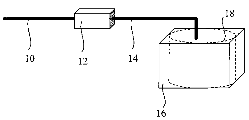
[0061] In this embodiment, the fluorine-containing plasma is generated in the process chamber that needs pretreatment, and depends on the excitation source of the process chamber to stimulate the ionization of the fluorine-containing gas passing into the process chamber to generate plasma; then, use the plasma to The inner wall of the process chamber and internal components are fluorinated. In the method, the in-situ fluorination treatment is performed after the plasma is generated, the process is simple, and the implementation is convenient. Moreover, the formed aluminum fluorine compound barrier layer has good uniformity in thickness and density, and high adhesion performance.

[0062] As a specific example, the fluorine-containing gas that passes into the process chamber can be CF4, and the flow rate is 500sccm to 1000sccm, and it can certainly be other fluorocarbons; the radio frequency source of the process chamber (in this implementation, the excitation source is a radio...


PUM

PropertyMeasurementUnit
Thicknessaaaaaaaaaa

Abstract

The invention relates to a method for pretreating a technical cavity of a plasma device, which is applied to the aluminous inner wall or the surface of an interior part of the technical cavity to form a protective layer. The invention comprises the steps of: carrying out fluorization on the inner wall and the surface of an interior part with plasma containing fluorine, and forming an aluminum fluorine compound barrier layer at the inner wall and the surface of an interior part. The aluminum fluorine compound formed by the invention has strong binding force with the inner wall of the technical cavity and the interior part, the size of the binding force of all parts is basically same, the corrosion resistance of the plasma is increased, particulate pollutant can be avoided or reduced, and compared with a spraying method, the invention has low cost and reduced manufacture difficulty.

Description

technical field [0001] The invention relates to the technical field of semiconductors, in particular to a pretreatment method for a process chamber of a plasma device. Background technique [0002] Dry etching machines, ion implanters, and chemical vapor deposition (CVD) equipment are important equipment used in the integrated circuit manufacturing process. In the above-mentioned equipment, the process gas mainly composed of halogen elements is introduced into the process chamber, and the ionization of the process gas is excited by the excitation source to form high-density plasma, which is used to treat the semiconductor substrate or structure in the process chamber. For processing; for example, in the dry etching process, plasma is used to etch patterns on semiconductor substrates or structures; in chemical vapor deposition processes, plasma-assisted deposition is used to form dielectric or metal film layers; in ion implantation In the process, the substrate is doped by i...

Claims


Application Information

Patent Timeline
IPC IPC(8): H01L21/00C23C16/44C23F4/00H01J37/32H01J37/317
Inventor 陶林
Owner BEIJING NAURA MICROELECTRONICS EQUIP CO LTD
Why Eureka
Try Eureka