Silicon-on-insulator lateral insulated gate bipolar transistor and process manufacturing method

A technology of silicon-on-insulator and bipolar transistors, which is applied in semiconductor/solid-state device manufacturing, semiconductor devices, electrical components, etc., can solve the problem of silicon-eating, severe, and inability to accurately control the depth and concentration distribution of N-type doping buffers, etc. problem, to achieve the effect of increasing the lateral breakdown voltage

Active Publication Date: 2010-06-30
SUZHOU POWERON IC DESIGN
View PDF0 Cites 9 Cited by
  • Summary
  • Abstract
  • Description
  • Claims
  • Application Information

AI Technical Summary

Problems solved by technology

[0004] In order to further increase the breakdown voltage of SOI-LIGBT, the improved structure adopts the method of extending the length of the polysilicon gate so that it covers the second-order field oxide layer to form a second-order field plate structure. This method has a certain effect. In related technologies, the formation of the second-stage field oxide layer is directly grown through thermal oxidation, and then formed through an etching process. However, the phenomenon of "silicon eating" in this process is very serious, which affects the surface morphology and surface area of ​​the drift region. concentration distribution
At the same time, in order to prevent SOI-LIGBT from punching through the anode, the improved structure will be provided with an N-type doped buffer zone 8 on the left side of the N-type doped drift region 6 (such as figure 1 shown), in the related art, the formation of the N-type doped buffer zone is completed by ion implantation before forming the P-type doped anode contact region 9, and then annealed, but this process method cannot accurately control the N-type Depth and concentration distribution of doping buffer

Method used


Image

  • Silicon-on-insulator lateral insulated gate bipolar transistor and process manufacturing method
  • Silicon-on-insulator lateral insulated gate bipolar transistor and process manufacturing method
  • Silicon-on-insulator lateral insulated gate bipolar transistor and process manufacturing method

Examples


Embodiment Construction

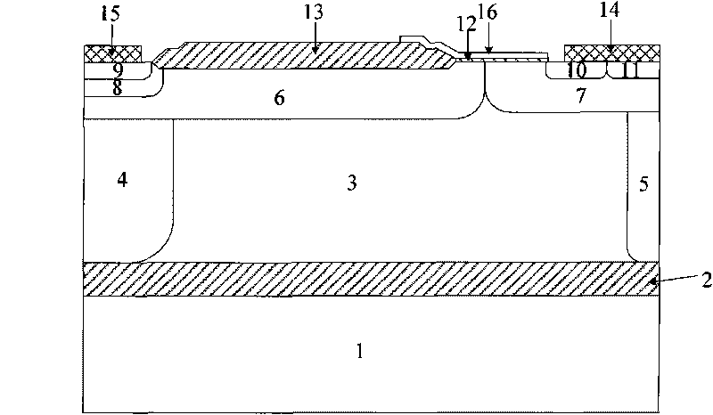
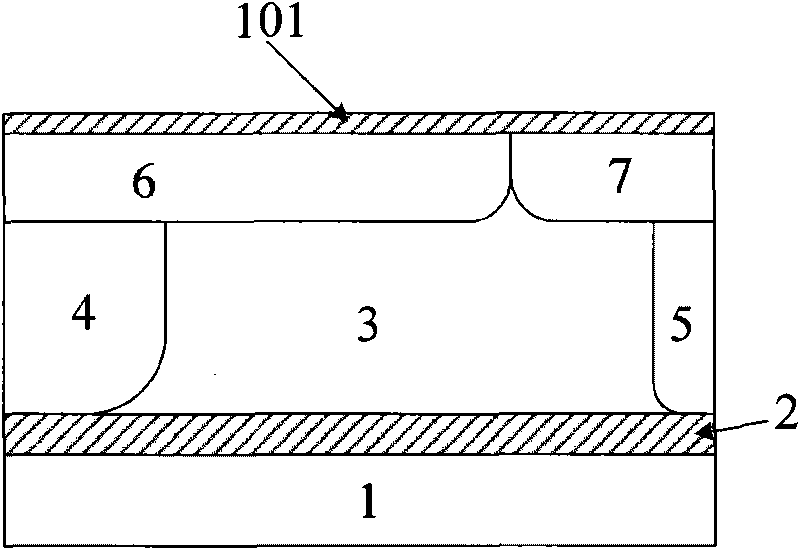
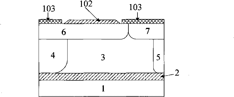
[0015] refer to figure 1 , a silicon-on-insulator lateral insulated gate bipolar transistor, comprising: a P-type doped semiconductor substrate 1, a buried oxide layer 2 is arranged on the P-type doped semiconductor substrate 1, and a P-type The doped epitaxial layer 3 is provided with an N-type doped deep well region 4 on the left side of the P-type doped epitaxial layer 3, and a P-type doped deep well region 5 is provided on the right side of the P-type doped epitaxial layer 3, An N-type doped drift region 6 is provided above the N-type doped deep well region 4 and part of the P-type doped epitaxial layer 3, and above the P-type doped deep well region 5 and part of the P-type doped epitaxial layer 3 A P-type doped semiconductor region 7 is provided. In the N-type doped drift region 6, an N-type doped buffer area 8 is arranged on the left side, and a P-type doped anode contact region 9 is arranged in the N-type doped buffer area 8, and in the P-type doped semiconductor regio...


PUM


Abstract

The invention discloses a process manufacturing method of a silicon-on-insulator lateral insulated gate bipolar transistor, comprising a P-type doped semiconductor substrate, a buried oxide layer is arranged on the P-type doped semiconductor substrate, an oxide layer is provided with an N-type drift region, a field oxide layer of the silicon-on-insulator lateral insulated gate bipolar transistor belongs to a second-order field oxide layer, and a field board which is formed by a gate extending to the above of the field oxide layer is a second-order field board. The second-order field oxide layer is formed by the steps of depositing the oxide layer, etching and thermal growth. An N-type doped buffer region is formed by implanting high-energy ions for self-alignment of the second-order field oxide layer.

Description

technical field [0001] The invention belongs to the technical field of integrated circuits, and relates to a manufacturing method of a lateral high-voltage power device, more specifically, to a lateral insulated gate bipolar transistor with silicon-on-insulator and a manufacturing method thereof. Background technique [0002] An insulated gate bipolar transistor (IGBT) is a device that has the advantages of an insulated gate structure of a metal oxide semiconductor (MOS) transistor and the advantages of high current density of a bipolar transistor. It is a device that can be used to effectively reduce the traditional Power MOSFET (Metal Oxide Semiconductor Field Effect Transistor) is a power semiconductor device with conduction loss. [0003] In order to be able to integrate with other semiconductor devices, Lateral Insulated Gate Bipolar Transistor (LIGBT) has received extensive attention and rapid development. Similarly, this device has high input impedance, high withstand...

Claims


Application Information

Patent Timeline
Patent Type & Authority Applications(China)
IPC IPC(8): H01L29/739H01L29/06H01L21/331H01L21/316H01L21/265
Inventor 易扬波李海松王钦刘侠陈文高陶平
Owner SUZHOU POWERON IC DESIGN
Why Eureka
Try Eureka