Method for preparing single-layer graphene film on SiO2 substrate directly

A single-layer graphite, direct technology, applied in the field of preparing two-dimensional nanomaterial single-layer graphene sheets directly on SiO2 substrates, can solve the problem of losing the properties of single-layer graphene layers, graphene sheets with many chemical impurities, and sheet Strong interaction with the substrate and other issues, to achieve the effect of low pressure, low cost and tight combination

A single-layer graphite, direct technology, applied in the field of preparing two-dimensional nanomaterial single-layer graphene sheets directly on SiO2 substrates, can solve the problem of losing the properties of single-layer graphene layers, graphene sheets with many chemical impurities, and sheet Strong interaction with the substrate and other issues, to achieve the effect of low pressure, low cost and tight combination

CN101768012AInactive Publication Date: 2010-07-07THE NAT CENT FOR NANOSCI & TECH NCNST OF CHINA

Image

  • Method for preparing single-layer graphene film on SiO2 substrate directly
  • Method for preparing single-layer graphene film on SiO2 substrate directly
  • Method for preparing single-layer graphene film on SiO2 substrate directly

Examples


Embodiment 1

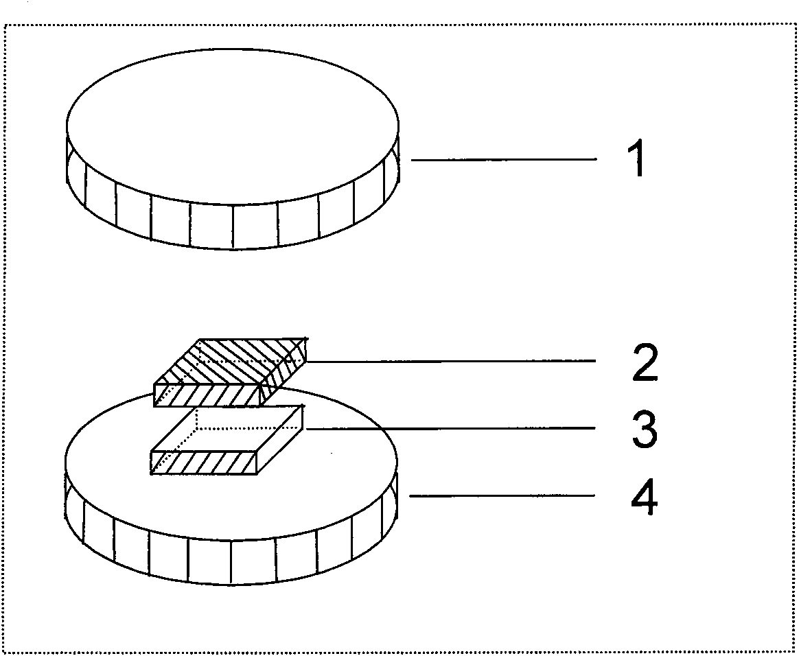
[0032] refer to figure 1 , to describe in detail the process flow of the method for preparing single-layer graphene by mechanical pressure of the present invention.

[0033] The preparation process of this embodiment is as follows:

[0034] 1). Prepare two flat, (111) crystal-oriented silicon wafers with a size of 10cm×10cm of 300nm thick silicon dioxide layer evaporated, one as the substrate, and the second as the backing plate in step 2); use Ultrasonic cleaning with acetone twice, the first time for 10 minutes, the second time for 5 minutes to make the surface clean; then ultrasonic cleaning with ethanol for 5 minutes to remove acetone molecules; ultrasonic cleaning with deionized water for 5 minutes to remove ethanol molecules; finally High-intensity cleaning with oxygen plasma for 5 minutes to remove molecules adsorbed on the surface;

[0035] 2). Take a block of grade A highly oriented pyrolytic graphite (HOPG) with a size of 10cmX10cmX2cm, use a sharp blade to cleava...

Embodiment 2

[0046] 1. Prepare a flat, 90nm-thick silicon dioxide layer evaporated, 10cmX10cm size (111) crystal-oriented silicon wafer as the substrate; clean it twice with acetone ultrasonically, the first time is 10 minutes, and the second time is 5 minutes , to make the surface clean; then ultrasonic cleaning with ethanol for 5 minutes to remove acetone molecules; ultrasonic cleaning with deionized water for 5 minutes to remove ethanol molecules; finally, high-intensity oxygen plasma cleaning for 5 minutes to remove surface-adsorbed molecules;

[0047] In order to further clean the substrate, it is also possible to perform a chemical solution immersion rinse before ultrasonic cleaning, that is, the cleaning process in the conventional semiconductor manufacturing process, such as soaking with acetone or isopropanol organic cleaning solution for 3-5 minutes, and then using ethanol Solution flushing;

[0048] 2. Take a block of grade A highly oriented pyrolytic graphite (HOPG) with a size...

Embodiment 3

[0057] Press the preparation method of embodiment 1, just change the pressure size into 15kg, change the time of keeping pressure into 5 minutes. The resulting graphene is similar. A mica sheet is selected as a backing plate, and it is cleaned and used by the cleaning process in the conventional semiconductor manufacturing process.


PUM

PropertyMeasurementUnit
thicknessaaaaaaaaaa

Abstract

The invention relates to a method for preparing two-dimensional nanomaterial single-layer graphene film on SiO2 substrate directly, comprising (1) preparing substrate and conducting purification treatment; (2) processing block-shaped highly-oriented pyrolytic graphite or natural flake-shaped graphite; (3) preparing the single-layer graphene film sample through mechanical compression method: adjusting pressure within 10kg-20kg, keeping pressure within 5-10min, then releasing the pressure, removing the block-shaped graphite, and taking out the silicon substrate to obtain the single-layer graphene film sample. The method for preparing the single-layer graphene film uses fewer devices, has low cost and high successful rate, and is easy to implement. The raw material is directly contacted with the substrate, accordingly, the pollution to the sample caused by the introduction of other auxiliary media can be avoided. The obtained graphene sample is of a complete sheet shape due to effect of pressure, without folds.

Description

technical field [0001] The present invention relates to a kind of preparation method of two-dimensional nanometer material single-layer graphene, relate to a kind of directly in SiO 2 A method for preparing a two-dimensional nanomaterial single-layer graphene sheet on a substrate. Background technique [0002] Single-layer graphene (graphene) is sp between carbon atoms 2 Hybridized into bonds, arranged in a two-dimensional honeycomb lattice single atomic layer planar crystal. A common material, graphite, is made up of layers of graphene sheets. For a long time, it has been theoretically believed that single-layer graphene is thermodynamically unstable and cannot exist stably in nature. [0003] In 2004, scientists from the University of Manchester in the United Kingdom prepared single-layer graphene in the laboratory for the first time, such as document 1: Novoselov, K.S.et al.Science 306, 666 (2004); Novoselov, K.S.et al.Proc.Natl.Acad.Sci .USA 102, 10451 (2005) introdu...

Claims


Application Information

Patent Timeline
07 Jul 2010
Publication
CN101768012A
IPC
C04B41/50; C04B41/52
Inventors
邱彩玉; 周海青