Al technical title is built by PatSnap Al team. It summarizes the technical point description of the patent document.
A nanostructure and hard template technology, applied in optics, optomechanical equipment, instruments, etc., can solve the problems of high cost, long preparation cycle of nanoscale imprint template, cost constraints of nanoimprint, etc.
Inactive Publication Date: 2010-07-07
SHANGHAI NANOTECH PROMOTION CENT +1
View PDF0 Cites 16 Cited by
Summary
Abstract
Description
Claims
Application Information
AI Technical Summary
This helps you quickly interpret patents by identifying the three key elements:
Problems solved by technology
Method used
Benefits of technology
Problems solved by technology
However, since the current high-precision imprint templates mainly rely on technologies such as electron beam direct writing, the preparation cycle of nanoscale imprint templates is long and the cost is high. A nanoscale template of 1 square centimeter will cost at least three to four months and hundreds of thousands of RMB. High cost severely restricts nanoimprint research
Method used
Image
Click on the blue label to locate the original text in one second.
Reading with bidirectional positioning of images and text.
Examples
Embodiment 1
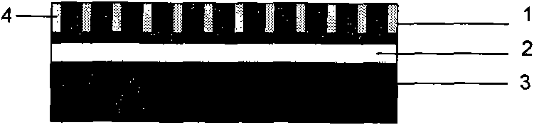
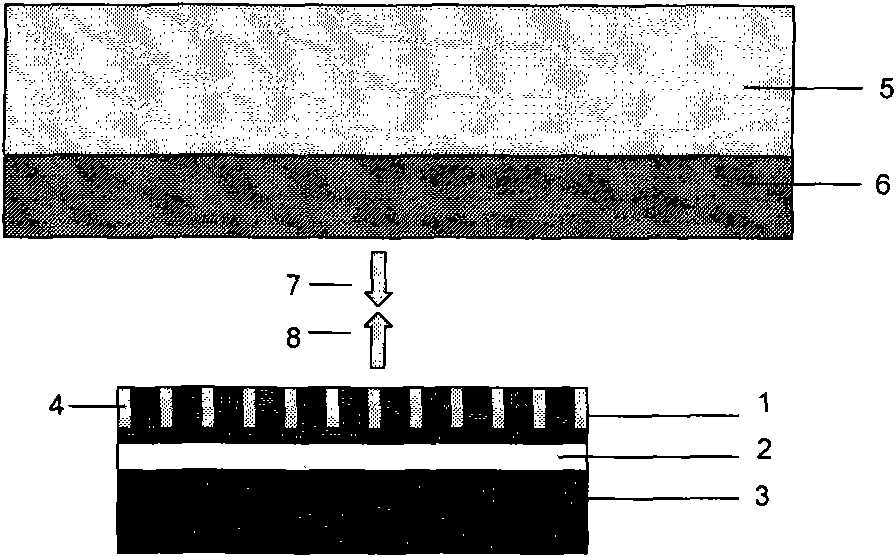
[0023] 1. First, deposit a layer of titanium with a thickness of 1 μm on the surface of 1 mm thick 2 inch quartz glass by sputtering.
[0024] 2. Next, cover a layer of aluminum on the surface of the titanium layer by evaporation, with a thickness of 10 μm. Made into a hard material base ( figure 1 ).
[0025] 3. Using the hard material substrate as the anode, the porous template ( figure 2 ), control the anodic oxidation reaction to terminate at the aluminum / titanium interface, soak in 5% (volume fraction) phosphoric acid to remove the barrier layer, and then use RIE to etch under the conditions of CF4 (15sccm) / AR (75sccm) mixed gas and power 210W 100s, remove the titanium layer at the bottom of the alumina hole.
[0026] 4. Carry out modification treatment by vapor deposition method, the modifier is CF3-(CF2)7-(CH2)2-SiCl3.
[0027] 5. The nanoscale high-density array structure was replicated on the surface of the silicon substrate by the cold imprinting process ( ima...
Embodiment 2
[0029] 1. First, a layer of chromium is deposited by sputtering on the surface of 0.5 mm thick 2-inch quartz glass, with a thickness of 2 μm.
[0030] 2. Then cover a layer of aluminum on the surface of the chromium layer by evaporation method, with a thickness of 100 μm. Made into a hard material base ( figure 1 ).
[0031] 3. Using the hard material substrate as the anode, the porous template ( figure 2 ), the thickness of the aluminum layer left at the bottom of the alumina hole is controlled at 10 μm.
[0032] 4. Use low-pressure spraying method for modification treatment to form a layer of modification film to reduce its surface energy. The modifier is CF3-(CF2)7-(CH2)2-SiCl3.
[0033] 5. Replicate a high-density structure on the surface of the silicon substrate using a hot embossing process ( image 3 , Figure 4 ).
PUM
Property
Measurement
Unit
thickness
aaaaa
aaaaa
thickness
aaaaa
aaaaa
pore size
aaaaa
aaaaa
Abstract
The invention relates to an impressing hard template in a nanostructure, which belongs to the field of nano manufacturing and is characterized in that a porous template with a hard material substrate is prepared by the porous AAO (anodic aluminum oxide) membrane technology and can be directly used as an impressing (from top to bottom) template after the hard substrate is added and the surface modification treatment is carried out. A porous AAO membrane can self-organize and grow into an ordered six-site symmetrical porous structure, and steep holes are uniformly distributed. When the porous AAO membrane is used as the template, various nanostructures and devices with optical, electrical and magnetic properties can be prepared by a processing method of directional assembling from bottom to top such as thermal evaporation, sputtering, deposition and electrochemical assembling. As the hard material substrate is added and the surface modification treatment is carried out, the AAO template technology is transplanted into the field of top-to-bottom surface micro-structure processing. Compared with the present technical method of the common electron beam direct writing, the manufacturing method for the impressing hard template with a nano-grade high-density structure not only has the obvious characteristics of low cost, short period and simple processing, but also can be widely used in the processing as well as researching of the nano-grade high-density surface nanostructure and particularly has broad prospects in the fields of semiconductor lighting and high-density storage. Meanwhile, as the hard substrate is increased, the shortcomings of the present brittle and fragile AAO template are overcome, thereby being more beneficial for duplication of the soft template.
Description
technical field [0001] The invention relates to a nanostructure embossing hard template, which belongs to the field of nanomanufacturing. Background technique [0002] With the reduction of chip feature size, traditional optical lithography is facing tremendous pressure from cost and technology, while nanoimprint technology has highlighted its strong competitiveness in the field of nano-processing with its outstanding advantages of low cost, high efficiency, and simplicity. and broad application prospects. Nano-imprint technology uses a template with nano-patterns to press the polymer film on the substrate out of nano-scale patterns, and then performs conventional etching, peeling and other processing on the imprinted parts, and finally makes nano-structures and devices. This technology can Nanostructures are prepared on large-area substrates repeatedly in large batches, and the high-resolution patterns produced have good uniformity and repeatability, are easily compatible ...
Claims
Application Information
Patent Timeline
Application Date:The date an application was filed.
Publication Date:The date a patent or application was officially published.
First Publication Date:The earliest publication date of a patent with the same application number.
Issue Date:Publication date of the patent grant document.
PCT Entry Date:The Entry date of PCT National Phase.
Estimated Expiry Date:The statutory expiry date of a patent right according to the Patent Law, and it is the longest term of protection that the patent right can achieve without the termination of the patent right due to other reasons(Term extension factor has been taken into account ).
Invalid Date:Actual expiry date is based on effective date or publication date of legal transaction data of invalid patent.