Liquid crystal display, liquid crystal display substrate and formation method thereof

A liquid crystal display and substrate technology, applied in the direction of instruments, semiconductor devices, electric solid devices, etc., can solve problems such as abnormal signals, water stains on the display, etc., to reduce static electricity or contact resistance, avoid burning phenomena, and avoid corrosion problems Effect

Active Publication Date: 2010-07-07
SHANGHAI TIANMA MICRO ELECTRONICS CO LTD
View PDF4 Cites 7 Cited by
  • Summary
  • Abstract
  • Description
  • Claims
  • Application Information

AI Technical Summary

Problems solved by technology

[0010] The problem to be solved by the present invention is to provide a liquid crystal display, a liquid crystal display substrate and its forming method, to prevent water stains, abnormal signals or burnt phenomena caused by uneven brightness of the display, and to prevent misjudgment of product defects

Method used


Image

  • Liquid crystal display, liquid crystal display substrate and formation method thereof
  • Liquid crystal display, liquid crystal display substrate and formation method thereof
  • Liquid crystal display, liquid crystal display substrate and formation method thereof

Examples


Embodiment Construction

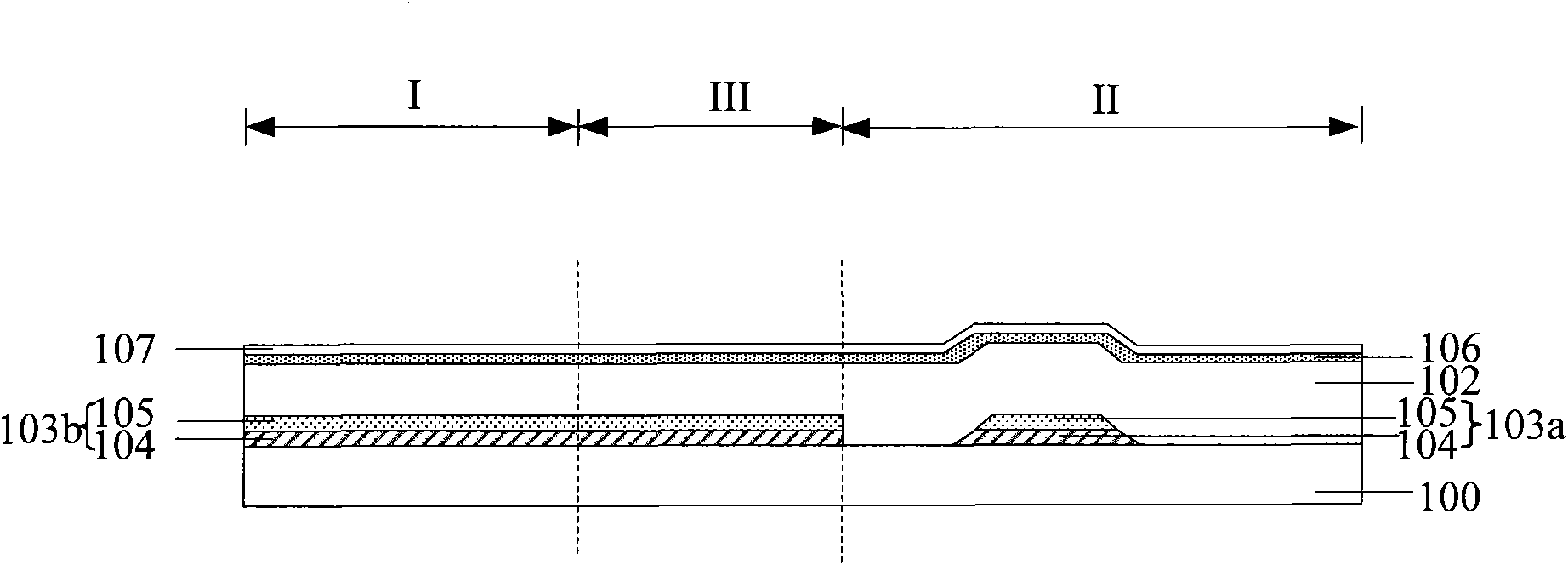
[0023] The invention adopts a single layer of aluminum or aluminum alloy as the material of the grid and the grid metal layer, which reduces the deposition steps, improves the production capacity, and effectively solves the problem that the use of two layers of metal film will produce a primary battery when the grid is formed by wet etching. The reaction leads to corrosion and the phenomenon of water marks caused by uneven brightness of the display.

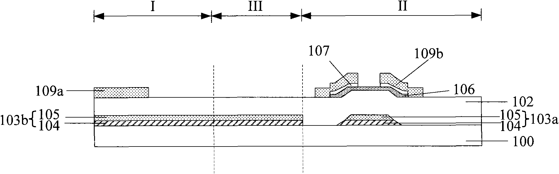
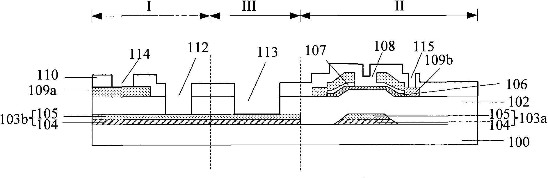
[0024] After the source / drain metal layer is connected to the gate metal layer, a passivation layer is deposited, and only the passivation layer is etched during the etching process, which can avoid the source / drain contact holes with different depths caused by etching in the prior art. The problem of over-etching of the drain metal layer; the surface of the source / drain metal layer connected to the gate metal layer in the present invention is flat, without damage caused by the etching problem, and improves the reliability of the ...


PUM

PropertyMeasurementUnit
thicknessaaaaaaaaaa
thicknessaaaaaaaaaa
thicknessaaaaaaaaaa

Abstract

The invention relates to a liquid crystal display, a liquid crystal display substrate and a formation method thereof. The method for forming the liquid crystal display substrate comprises the following steps: forming a gate metal layer in a short-circuiting bar area and a pad area on a substrate and forming a gate electrode in a pixel unit area; sequentially forming a gate electrode insulation layer and an amorphous silicon composite layer which cover the gate metal layer and the gate electrode on the substrate; etching the amorphous silicon composite layer and the gate electrode insulation layer in the short-circuiting bar area and the pad area until the gate metal layer is exposed to form a short-circuiting bar area contact hole and a pad area contact hole; etching the amorphous siliconcomposite layer and reserving the amorphous silicon composite layer at a position corresponding to the gate electrode in the pixel unit area; forming a source/drain electrode metal layer on the gate electrode and the amorphous silicon composite layer and in the short-circuiting bar area contact hole and the pad area contact hole; and etching the source/drain electrode metal layer to form a source/drain electrode and a conducting channel in the pixel unit area and electrically connect the gate electrode metal layer with the source/drain electrode metal layer in the short-circuiting bar area. The liquid crystal display and the liquid crystal display substrate and the formation method thereof improve the reliability of a device and the efficiency of product quality analysis.

Description

technical field [0001] The invention relates to the technical field of TFT-LCD (thin film transistor liquid crystal display) manufacture, in particular to a liquid crystal display, a liquid crystal display substrate and a forming method thereof. Background technique [0002] Currently, a liquid crystal unit of a liquid crystal display usually includes an upper substrate and a lower substrate, and a TFT circuit is formed on one of the substrates. [0003] The formation process of the existing liquid crystal display substrate is specifically as follows: figure 1 As shown, a substrate 100 including pad region III, pixel unit region II and shorting bar region I is provided; a gate 103a is formed on the substrate of pixel unit region II, and a substrate of pad region III and shorting bar region I is formed. A gate metal layer 103b is formed on the bottom 100, and the gate 103a and the gate metal layer 103b are laminated by an aluminum or aluminum alloy layer 104 and a metal moly...

Claims


Application Information

Patent Timeline
Patent Type & Authority Applications(China)
IPC IPC(8): H01L21/82H01L21/768H01L27/02H01L23/52G02F1/1362
Inventor 张根夏张容
Owner SHANGHAI TIANMA MICRO ELECTRONICS CO LTD
Why Eureka
Try Eureka