Programmable TVS apparatus with low capacitance and low voltage

A low-capacitance, device technology, applied in the field of low-capacitance voltage programmable TVS devices, can solve the problems that TVS has not yet been launched, and achieve the effect of low clamping, low device capacitance, and lower clamping voltage

Active Publication Date: 2014-03-05
SHANGHAI CHANGYUAN WAYON MICROELECTRONICS
View PDF4 Cites 0 Cited by
  • Summary
  • Abstract
  • Description
  • Claims
  • Application Information

AI Technical Summary

Problems solved by technology

But on low-voltage terminal equipment, TVS for programmable applications has not yet been launched

Method used


Image

  • Programmable TVS apparatus with low capacitance and low voltage
  • Programmable TVS apparatus with low capacitance and low voltage
  • Programmable TVS apparatus with low capacitance and low voltage

Examples


Embodiment 1

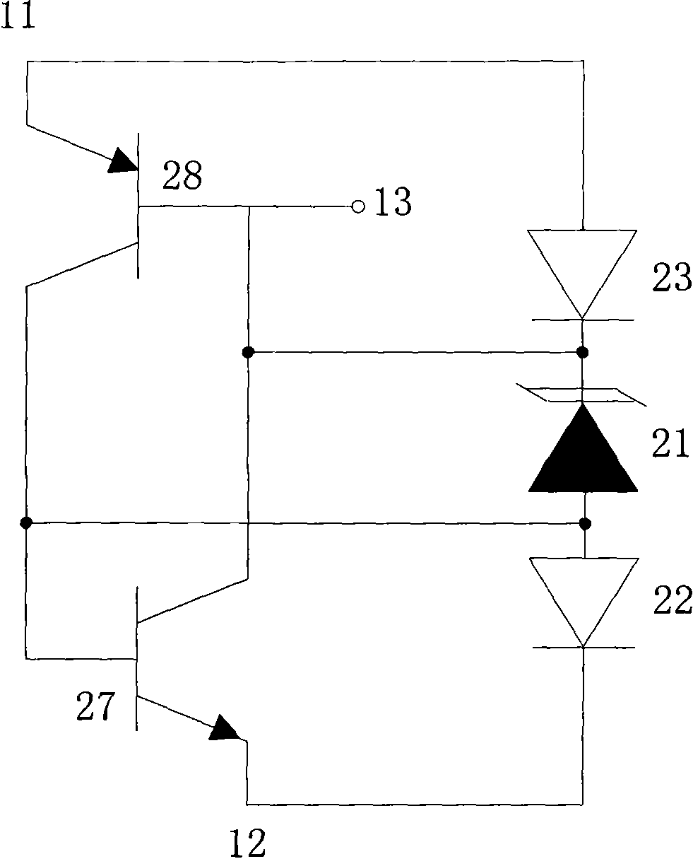
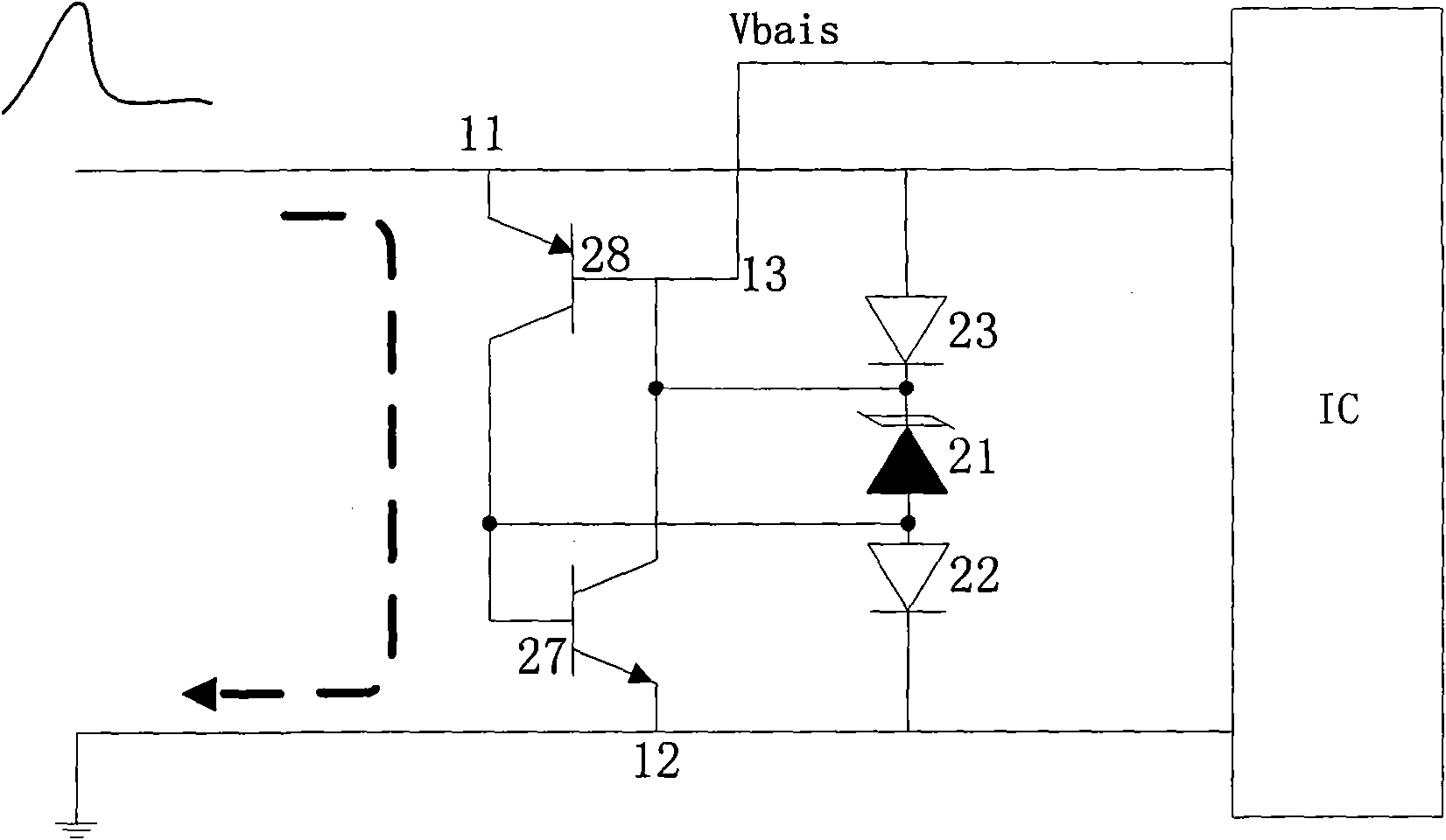
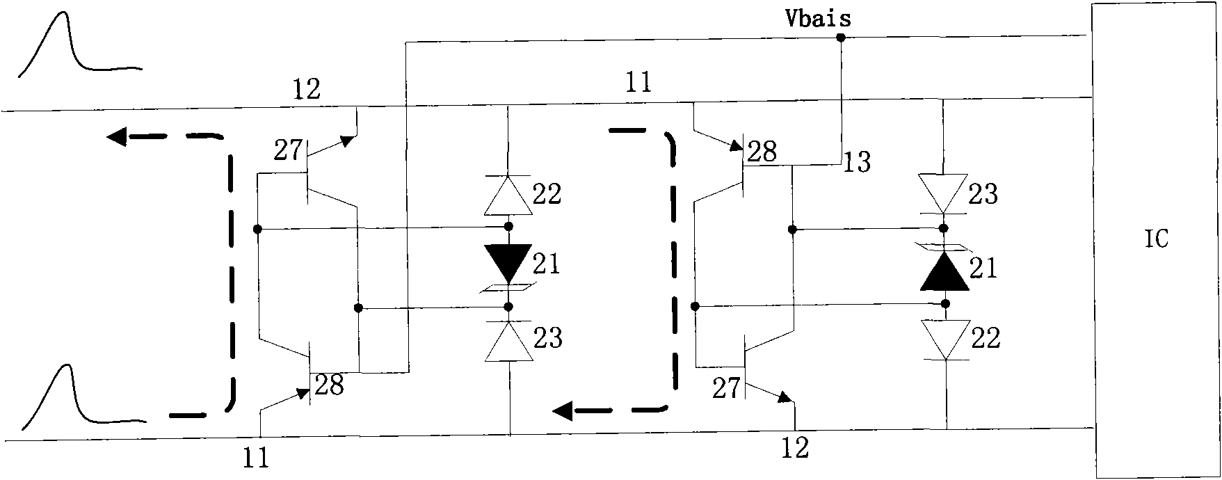
[0095] see figure 1 As shown in the circuit schematic diagram of the TVS device in Embodiment 1 of the present invention, a low-capacitance voltage programmable TVS device is composed of a latch path and a voltage-limiting protection path of a low-capacitance diode. The TVS device is composed of a PNP transistor and an NPN transistor. Composed of TVS tubes, used for programmable protection, low capacitance and limited protection voltage upper limit, among which:

[0096] On the latch path, the PNP transistor 28 and the NPN transistor 27 form a latch structure, the input terminal 11 is connected to the emitter of the PNP transistor 28, the collector of the PNP transistor 28 is connected to the base of the NPN transistor 27, and the base of the PNP transistor 28 is connected to The collector of the NPN transistor 27, the emitter of the NPN transistor 27 is connected to the output terminal 12, and the collector of the PNP transistor 28 is connected to the anode of the TVS tube 21, ...

Embodiment 2

[0121] see Figure 10 It is the circuit schematic diagram and the Figure 11 It is a schematic diagram of the side sectional structure of the TVS device in Embodiment 2 of the present invention, and other structures and manufacturing methods from the first step to the fourth step are the same as in Embodiment 1.

[0122] Step 5: Doping boron elements on the left side of the epitaxial layer 32a to make a P+ expansion region 24 to form the anode of the forward-directed diode 29 to form the ohmic contact of the gate electrode 13, and doping a phosphorus element on the right side to make an N+ contact region 44, forming an ohmic contact leading to the cathode of the diode 22;

[0123] Step 6: Deposit a metal layer on the surface of the device, and divide the metal layer into three parts by photolithography. The metal layer 33 on the left leads out the P+ expansion area 24 to form the gate 13 electrode, and the middle metal layer 34 separates the P+ expansion area 43 lead out to ...

Embodiment 3

[0125] see Figure 12 It is the circuit schematic diagram and the Figure 13 It is a schematic diagram of the side sectional structure of the TVS device in Embodiment 3 of the present invention, and other structures and manufacturing methods from the first step to the fifth step are the same as in Embodiment 1.

[0126] Step 6: Connect the polysilicon resistor 20 to the N+ contact area 46 on the left;

[0127] Step 7: Deposit a metal layer on the surface of the device, and divide the metal layer into three parts by photolithography. The metal layer 33 on the left leads out one end of the polycrystalline resistor 20 to form the gate 13 electrode, and the other end passes through the N+ contact area 46 In contact with the N- epitaxial layer 32, the middle metal layer 34 leads out the P+ expansion region 43 to form the electrode of the input terminal 11, and the right metal layer 35 leads out the right N+ contact region 44 to form the electrode of the output terminal 12.

[012...


PUM


Abstract

The invention relates to a programmable TVS apparatus with low capacitance and low voltage and a manufacturing method thereof. The programmable TVS apparatus consists of a latch access and a voltage-limiting protective access. In terms of the latch access, a PNP triode and a NPN triode form a latch structure. A gate pole of the apparatus is formed in such a way that the input end is connected with the emitting electrode of the PNP triode, the collecting electrode of the PNP triode is connected with the base electrode of the NPN triode, the base electrode of the PNP triode is connected with the collecting electrode of the NPN triode, the emitting electrode of the NPN triode is connected with the output end, the collecting electrode of the PNP triode is connected with the anode of the TVS tube, and the base electrode of the PNP triode is connected with the cathode of the TVS tube. In terms of the voltage-limiting access, the voltage-limiting access consists of two derating diodes and a TVS apparatus, wherein the anode of the TVS tube is connected with the anode of the first guide diode, the cathode of the TVS tube is connected with the cathode of the second guide diode, the anode of the second guide diode is connected with the input end, and the cathode of the first guide diode is connected with the output end. By changing the electric potential of the gate pole, programmable protection and over-voltage protection within the TVS breakdown voltage can be realized.

Description

technical field [0001] The invention relates to the field of semiconductor devices, in particular to a low-capacitance voltage programmable TVS device and a manufacturing method thereof. Background technique [0002] TVS devices are bidirectional low-voltage transient voltage suppression devices, which are widely used in surge and ESD protection of circuits. [0003] Under normal circumstances, the devices used for overvoltage protection on terminal equipment generally use TVS, varistor and other protection devices. The protection voltage of such devices is generally fixed, and it needs to be selected according to the size of the user's working voltage during use. , but in some cases, the operating voltage of the line is uncertain. In this case, we generally choose the highest operating voltage for surge or ESD protection. We know that this method actually has a hidden danger. Any overvoltage signal will affect its normal operation. [0004] To solve this problem, ST intro...

Claims


Application Information

Patent Timeline
Patent Type & Authority Patents(China)
IPC IPC(8): H01L27/07H01L21/77
Inventor 张关保苏海伟张婷叶力吴兴农
Owner SHANGHAI CHANGYUAN WAYON MICROELECTRONICS
Why Eureka
Try Eureka