LED (light-emitting diode) of zinc-oxide based transparent electrode and manufacturing method thereof
A technology of light-emitting diodes and transparent electrodes, which is applied in the direction of circuits, electrical components, semiconductor devices, etc., can solve the problems of complex process and long time consumption, and achieve the effect of simple preparation process, low cost and uniform current diffusion
- Summary
- Abstract
- Description
- Claims
- Application Information
AI Technical Summary
Problems solved by technology
Method used
Image
Examples
Embodiment 1
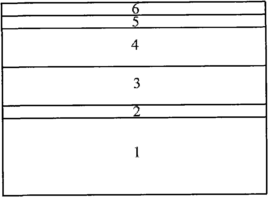
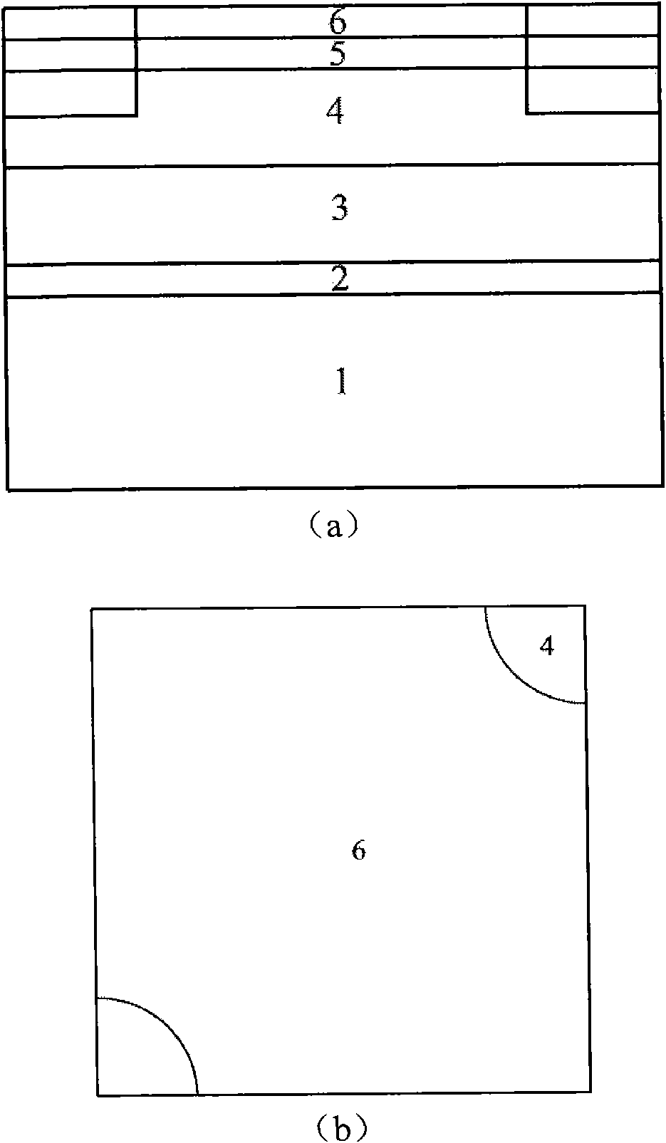
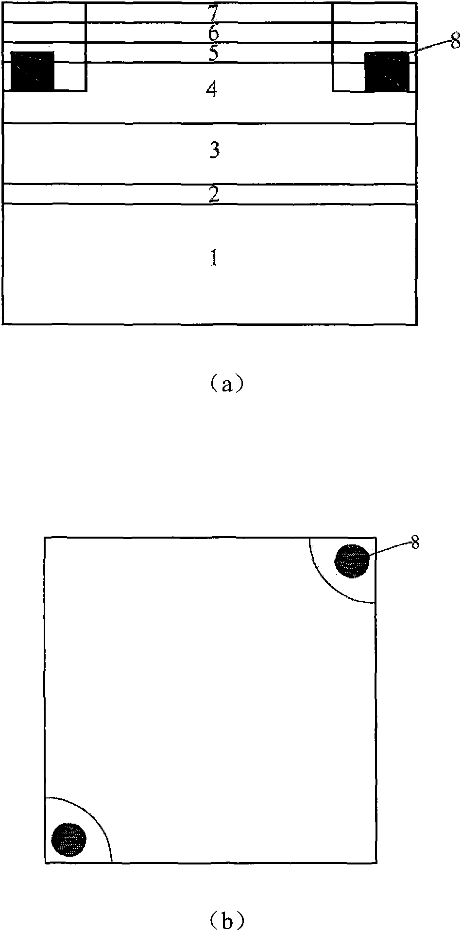
[0034] Embodiment one: see figure 1 , figure 2 , image 3 , Figure 4 , the zinc oxide-based transparent electrode light-emitting diode includes: sapphire substrate 1, buffer layer 2, intrinsic layer 3, n-type gallium nitride 4, quantum well 5, p-type gallium nitride 6, transparent electrode 7, n-type metal Electrode (PAD) 8, p-type metal electrode (PAD) 9. n-PAD is a Ti / Al or Cr / Pt / Au composite electrode, which is in the shape of a truncated cone on the opposite corner of the chip; p-PAD is a Ni / Au or Cr / Pt / Au composite electrode, which is in the shape of a small truncated cone or opposite Multi-crossing branches with diagonal distribution, or "I" shape with diagonal distribution. The transparent electrode is a zinc oxide-based transparent conductive film made of ZnO:Ga or ZnO:Al or ZnO:In;
Embodiment 2
[0035] Embodiment two: the manufacturing method of the zinc oxide-based transparent electrode light-emitting diode chip is as follows: first, buffer layer 2, intrinsic layer 3, n-type gallium nitride 4, quantum well 5, p-type Gallium nitride 6 and magnesium activation annealing treatment; secondly, use the photoresist as a pattern mask, and etch the epitaxial wafer by ICP dry etching method to expose the n-type gallium nitride; float the photoresist, Carry out pattern mask again, deposit zinc oxide transparent conductive thin film 7 by magnetron sputtering method; Again, deposit n-type metal electrode (PAD) 8 and p-type metal electrode (PAD) 9 by the method for thermal evaporation or electron beam evaporation ; Finally, carry out the alloying annealing treatment of the metal electrode and split the epitaxial wafer.
PUM
 Abstract
Description
Claims
Application Information
 - R&D
- Intellectual Property
- Life Sciences
- Materials
- Tech Scout
- Unparalleled Data Quality
- Higher Quality Content
- 60% Fewer Hallucinations
Browse by: Latest US Patents, China's latest patents, Technical Efficacy Thesaurus, Application Domain, Technology Topic, Popular Technical Reports.
© 2025 PatSnap. All rights reserved.Legal|Privacy policy|Modern Slavery Act Transparency Statement|Sitemap|About US| Contact US: help@patsnap.com


