MEMS atom cavity chip and preparation method thereof

An atomic cavity and chip technology, which is applied in the field of integrated atomic cavity chips and its preparation, can solve the problems of low integration, complex processing technology of thermally isolated atomic cavity, etc., and achieve the effects of improved isolation effect, shortened heating time, and high integration degree.

Inactive Publication Date: 2010-07-14
BEIHANG UNIV
View PDF0 Cites 34 Cited by
  • Summary
  • Abstract
  • Description
  • Claims
  • Application Information

AI Technical Summary

Problems solved by technology

[0003] Problems solved by the technology of the present invention: Overcoming the deficiencies of the prior art, adopting MEMS processing technology, providing a MEMS atomic cavity chip and its preparation method, so

Method used


Image

  • MEMS atom cavity chip and preparation method thereof
  • MEMS atom cavity chip and preparation method thereof
  • MEMS atom cavity chip and preparation method thereof

Examples


Embodiment Construction

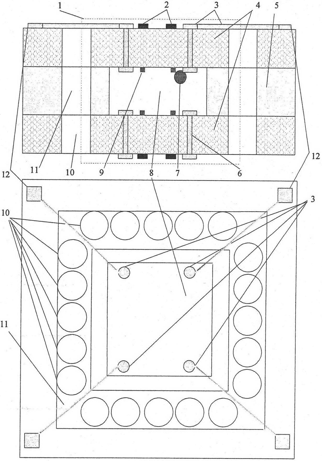
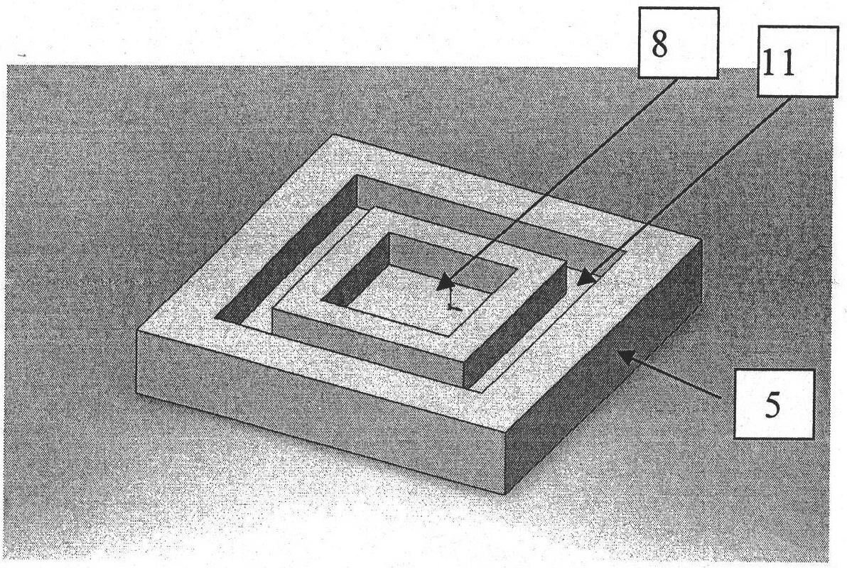
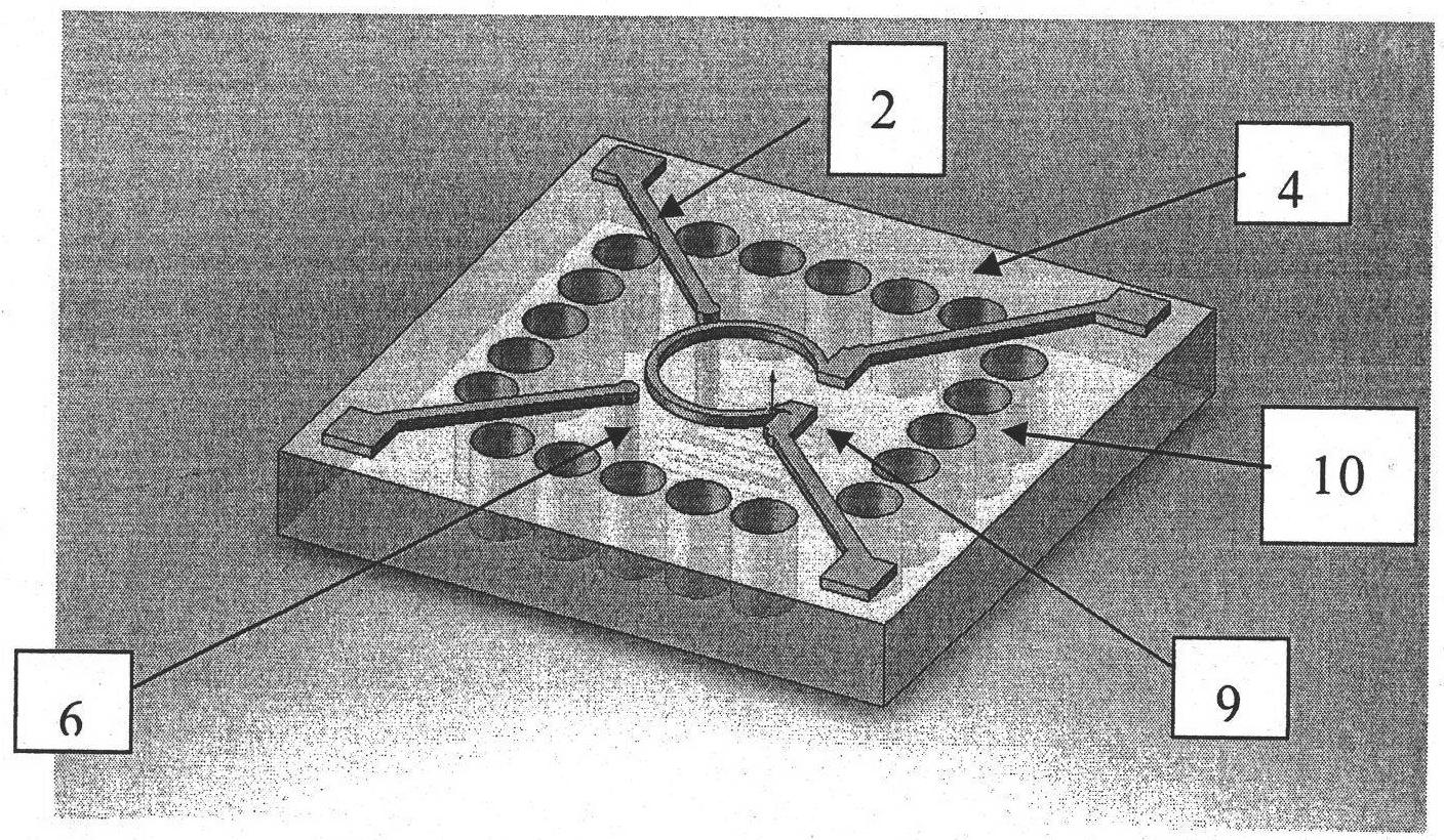
[0038] like figure 1 As shown, it is a structural schematic diagram of the MEMS atomic cavity chip of the present invention, including a radio frequency coil 2, an electrical connection lead 3, two glass substrates 4, a silicon substrate 5, an electrical connection through hole 6, an alkali metal 7, and a cavity space 8. Resistance heating wire 9, thermal isolation through hole 10, thermal isolation ring 11, pad 12, two glass substrates 4 and one silicon substrate 5 are bonded together to form a thermal isolation atomic cavity 1, namely figure 1 The box part indicated in is thermally isolated atomic cavity 1;

[0039] The two glass substrates 4 are identical in structure and symmetrical up and down. There are thermal isolation through holes 10 and electrical connection through holes 6 on the glass substrate 4. The electrical connection through holes 6 are filled with metal nickel, or other electroplatable metals. , such as copper, silver, etc. There are Cr / Au radio frequency...


PUM

PropertyMeasurementUnit
Diameteraaaaaaaaaa
Diameteraaaaaaaaaa

Abstract

The invention discloses an MEMS atom cavity chip and a preparation method thereof. The chip comprises two glass substrates and a silicon substrate, heater strips and radio-frequency coils are integrated on the glass substrates, metal leads connecting front faces and reverse faces are processed by laser perforation and plating technology. Atom cavity spaces and thermal insolating rings are integrated on the silicon substrate. The injection of alkalis is finished in an anaerobic box, the injection and bonding of air is finished then, and the injection of high concentration supplementary air is realized. The invention has high integrated level, and realizes on-chip integration of the heater strip, the radio-frequency coil and thermal isolating ring structures. The invention can be used for MEMS atomic gyroscopes besides MEMS atomic clocks and MEMS atom magnetometers.

Description

technical field [0001] The invention belongs to the field of micro-electromechanical system processing, and in particular relates to an integrated atomic cavity chip applicable to MEMS atomic gyroscopes and a preparation method thereof, which can be used for MEMS atomic clocks, MEMS atomic magnetometers and MEMS atomic gyroscopes. Background technique [0002] As an emerging high-tech field, micro-electro-mechanical systems (MEMS) use advanced semiconductor technology to integrate the entire mechanical structure into a chip, and have been widely used in military, biomedical, automotive and other industries. In recent years, with the development of atomic physics, laser diode technology and micro-nano manufacturing technology, a new research field of atomic MEMS has gradually formed. Atomic MEMS devices are characterized by high precision and small size compatibility. The current main devices include MEMS atomic clocks, MEMS atomic magnetometers and MEMS atomic gyroscopes. M...

Claims


Application Information

Patent Timeline
IPC IPC(8): B81B7/02B81C1/00B81C3/00
CPCG04F5/145
Inventor 董海峰房建成周斌权万双爱秦杰
Owner BEIHANG UNIV
Why Eureka
Try Eureka