Method for manufacturing back contact solar energy batteries

A technology for solar cells and manufacturing methods, applied in final product manufacturing, sustainable manufacturing/processing, circuits, etc., can solve problems such as high technical cost and difficulty in implementing P-type diffusion technology, and achieve process simplification, easy implementation, and cost reduction. Effect

Active Publication Date: 2010-07-14
BEIJING NAURA MICROELECTRONICS EQUIP CO LTD
View PDF0 Cites 51 Cited by
  • Summary
  • Abstract
  • Description
  • Claims
  • Application Information

AI Technical Summary

Problems solved by technology

[0008] The above existing technologies have at least the following disadvantages: P-type diffusion technology is difficult to realize and the technology cost is high

Method used


Image

  • Method for manufacturing back contact solar energy batteries
  • Method for manufacturing back contact solar energy batteries
  • Method for manufacturing back contact solar energy batteries

Examples


specific Embodiment

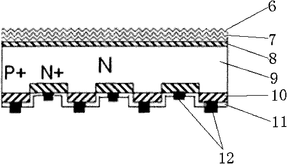
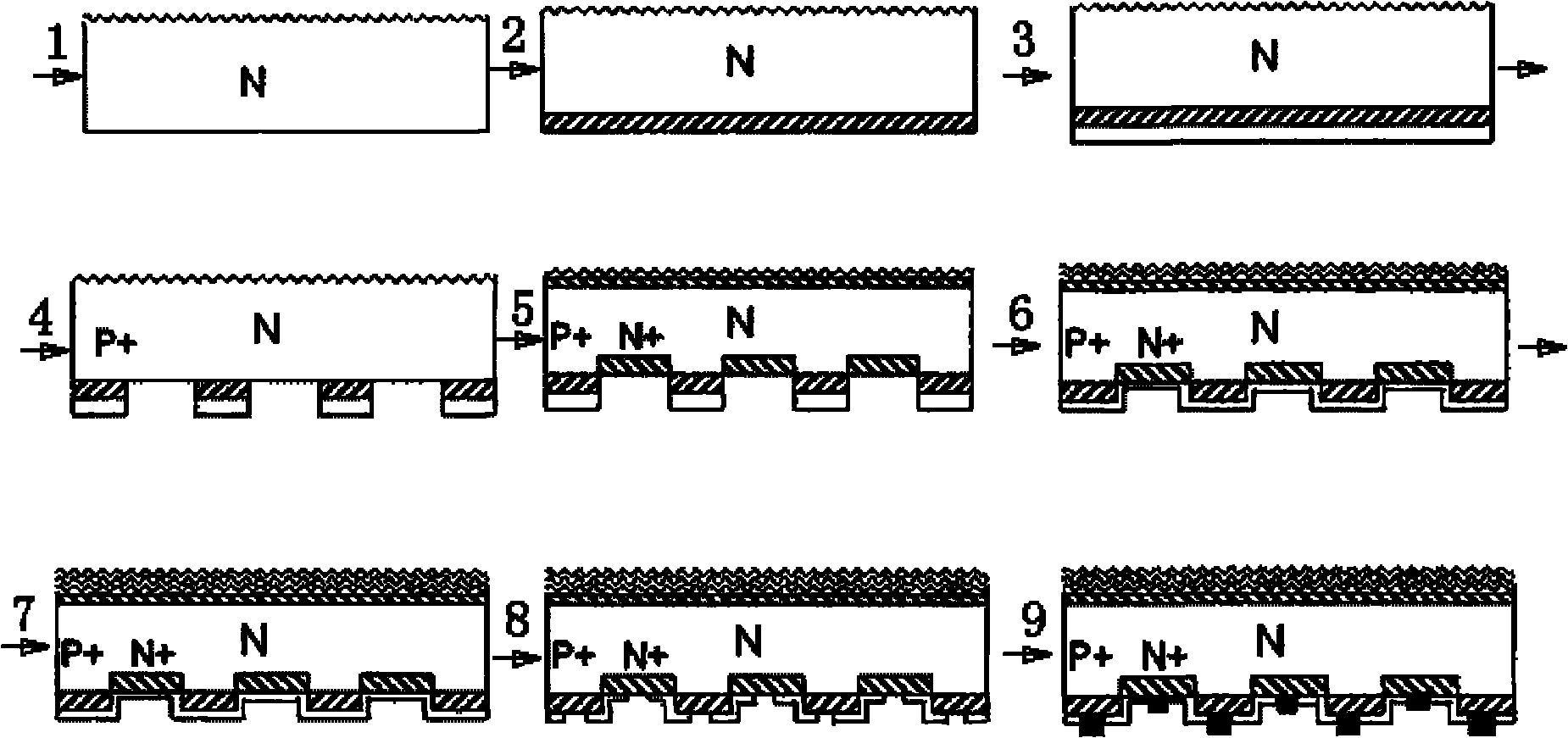
[0029] Specific examples, such as image 3 As shown, the process flow includes steps:

[0030] Step 1, silicon wafer cleaning, surface texture:

[0031] Zone-melting N-type monocrystalline silicon wafers with a thickness of 220-280um are selected as the base material, and the silicon wafers are cleaned with a NaOH solution with a mass fraction of 2%-15% and a temperature between 60°C and 90°C to remove the silicon wafers. The surface is damaged, and the front side of the silicon wafer is made into an inverted pyramid suede with a mixed solution of KOH and IPA (isopropanol).

[0032] Step 2, growing a P-type doped silicon dioxide layer:

[0033] A P-type doped layer is grown on the back of the substrate. The doping source can be boron or other P-type dopants. The P-type doped layer can be deposited by conventional techniques such as atmospheric pressure chemical vapor deposition and plasma enhanced chemical vapor deposition. Deposited by various deposition methods, the thick...


PUM


Abstract

The invention discloses a method for manufacturing back contact solar energy batteries, comprises the following steps of: firstly growing a P type doped silicon dioxide layer on an N type silicon chip; then growing a non-doped silicon dioxide layer on a P type doped layer; after that, printing a corrosive agent or an anti corrosive agent on the non-doped silicon dioxide layer to corrode the P type doped silicon dioxide layer and the non-doped silicon dioxide layer so as to form required patterns; and finally carrying out N type adulteration on the back face and the front face of the silicon chip to form an N type doped layer. The P type doped layer is protected by the non-doped silicon dioxide layer, and an N front surface field on the front face of the battery and a PN alternating doped layer on the back face of the battery are realized in the N type doped step at the same time, thereby reducing the diffusion step, reducing the cost and simplifying the process.

Description

technical field [0001] The invention relates to a solar cell manufacturing technology, in particular to a back contact solar cell manufacturing method. Background technique [0002] Solar cells are semiconductor devices that convert solar energy into electrical energy through the photovoltaic effect. They are mainly made of semiconductor materials. . The basic structure of a silicon solar cell is a PN junction. When light enters the cell, electron-hole pairs are generated due to the photoelectric effect. These minority carriers (hereinafter referred to as minority carriers) are accelerated by the built-in electric field of the PN junction and are positively and negatively The electrodes collect it as electrical energy and store it. [0003] like figure 1 As shown, in prior art 1, a traditional solar cell diffuses a layer of N-type doped layer 3 on the surface of P-type material 2 to form a PN junction. Electron-hole pairs (electron-hole) are generated on both sides of th...

Claims


Application Information

Patent Timeline
Patent Type & Authority Applications(China)
IPC IPC(8): H01L31/18
CPCY02P70/50
Inventor 肖青平
Owner BEIJING NAURA MICROELECTRONICS EQUIP CO LTD
Why Eureka
Try Eureka