Packaging structural element of dye-sensitized cell and packaging method thereof
The invention relates to a dye-sensitized battery and packaging method technology, which is applied to the packaging structure and packaging field of dye-sensitized batteries, and can solve the problems of poor lamination process stability and uniformity of sarin film, difficulty in ensuring packaging uniformity with glass paste, Problems such as poor stability of sarin film packaging process
- Summary
- Abstract
- Description
- Claims
- Application Information
AI Technical Summary
Problems solved by technology
Method used
Image
Examples
preparation example Construction
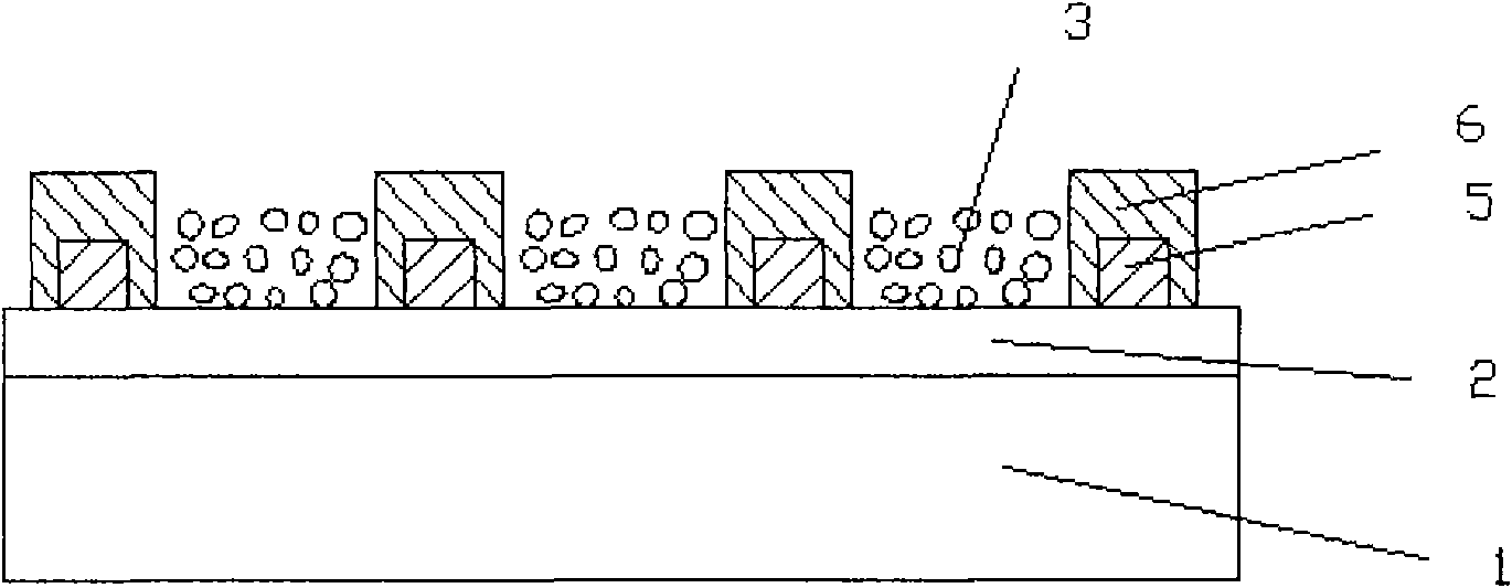
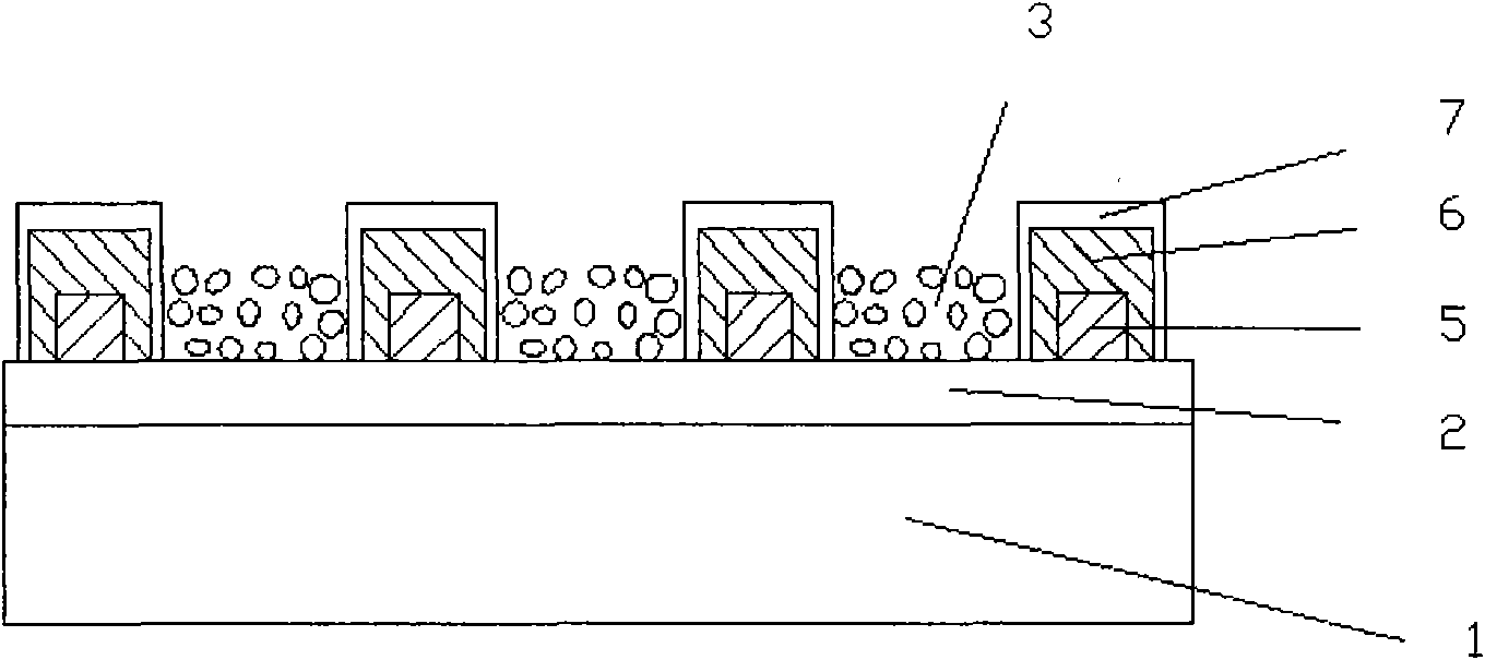
[0046] The preparation method of the packaging structure of the dye-sensitized battery of the present invention is described below. The packaging structure of the present invention is a packaging structure of two or more layers combined, which at least includes a layer covering the conductive electrode (5) A hard insulating layer (6) on the surface and an adhesive bonding layer (7) covering the surface of the hard insulating layer (6). The packaging structure in which the hard insulating layer (6) and the adhesive adhesive layer (7) covering the hard insulating layer (6) are combined is a kind of packaging structure that can effectively prevent battery Short-circuited packaging structure, because the adhesive is deformed under high temperature and pressure, the adhesive bonding layer is thinned, but the introduction of a hard insulating layer can effectively prevent the contact point between the photoanode and the conductive electrode on the counter electrode, thereby Prevent ...
Embodiment 1
[0082] The conductive electrode 5 is a silver electrode, and the hard insulating layer 6 is TiO 2 slurry, and when the hard insulating layer 6 is not sintered, the adhesive layer 7 is an adhesive layer formed by a common solvent-resistant thermal adhesive, such as JELCON AD-HM6 ink. The specific implementation method is:
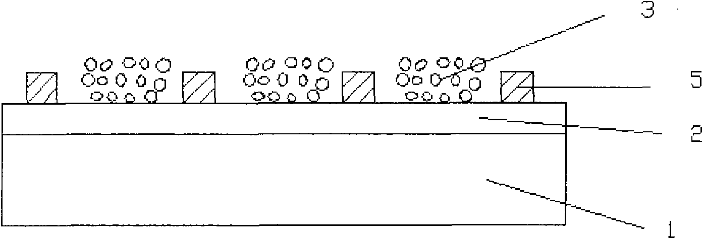
[0083] 1. In such as figure 1 On the photoanode assembly of the above-mentioned photoanode, the silver electrode 5 is covered with a layer of titanium dioxide slurry with a thickness of 9 microns by using a screen printing process, and dried at 125° C. for 8 minutes to obtain a hard insulating layer 6, that is, the following can be obtained: figure 2 The photoanode assembly shown. The mesh number of the wire mesh is 100 mesh.
[0084] 2. Next, use the screen printing process to print a layer of AD-HM6 ink adhesive layer with a thickness of 8 microns on the hard insulating layer 6, and cure it at 60°C for 2 minutes to obtain the adhesive adhesive layer 7,...
Embodiment 2
[0089] The conductive electrode 5 is (ACHESON) ED 581SS conductive carbon paste, and the hard insulating layer 6 is TiO 2 slurry, and when the hard insulating layer 6 is not sintered, the adhesive layer 7 is an adhesive layer formed by a common solvent-resistant thermal adhesive, such as JELCON AD-HM6 ink. The specific implementation method is:
[0090] 1. After adsorbing dyes such as Figure 5 On the photoanode assembly shown, use a screen printing process to print a layer of (ACHESON) ED 581SS conductive carbon paste with a thickness of 6 microns on the position of the conductive electrode, and cure it at 135°C for 60 minutes, and then you can get the following: figure 1 The photoanode assembly shown. Wherein the conductive electrode is ED 581SS conductive carbon paste. The number of wire mesh used is 200 mesh.
[0091] 2. Next, use the screen printing process to cover the conductive electrode with a layer of titanium dioxide slurry with a thickness of 9 microns as a har...
PUM
| Property | Measurement | Unit |
|---|---|---|
| thickness | aaaaa | aaaaa |
| thickness | aaaaa | aaaaa |
| melting point | aaaaa | aaaaa |
Abstract
Description
Claims
Application Information


