Introduction-type roughening nitrogen polar surface gallium nitride based light-emitting diode and manufacturing method thereof

A light-emitting diode, gallium nitride-based technology, applied in the direction of electrical components, circuits, semiconductor devices, etc., to achieve the effect of improving light extraction efficiency, maintaining electrical performance and manufacturing yield

Active Publication Date: 2010-08-18
XIAMEN SANAN OPTOELECTRONICS TECH CO LTD
View PDF4 Cites 7 Cited by
  • Summary
  • Abstract
  • Description
  • Claims
  • Application Information

AI Technical Summary

Problems solved by technology

[0004] Aiming at the problem that the above-mentioned gallium polar surface roughening and nitrogen polar surface roughening cannot be applied to conventional gallium nitride-based light-emitting diode chips, the present invention aims to provide an introductory roughened nitrogen polar surface gallium nitride-based light-emitting diode Its manufacturing method includes introducing a gallium nitride epitaxial layer with a roughened nitrogen polar surface through diffusion bonding and substrate removal on the basis of a conventional gallium nitride-based light-emitting diode chip structure, ensuring a substantial improvement in Under the premise of chip light extraction efficiency, the original electrical performance of the chip can be kept unchanged, and at the same time, the manufacturing yield equivalent to that of conventional gallium nitride-based light-emitting diodes can be obtained.

Method used


Image

  • Introduction-type roughening nitrogen polar surface gallium nitride based light-emitting diode and manufacturing method thereof
  • Introduction-type roughening nitrogen polar surface gallium nitride based light-emitting diode and manufacturing method thereof
  • Introduction-type roughening nitrogen polar surface gallium nitride based light-emitting diode and manufacturing method thereof

Examples


Embodiment Construction

[0046] The present invention will be further described below in conjunction with the accompanying drawings and embodiments.

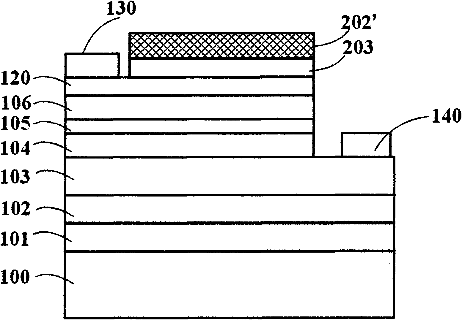
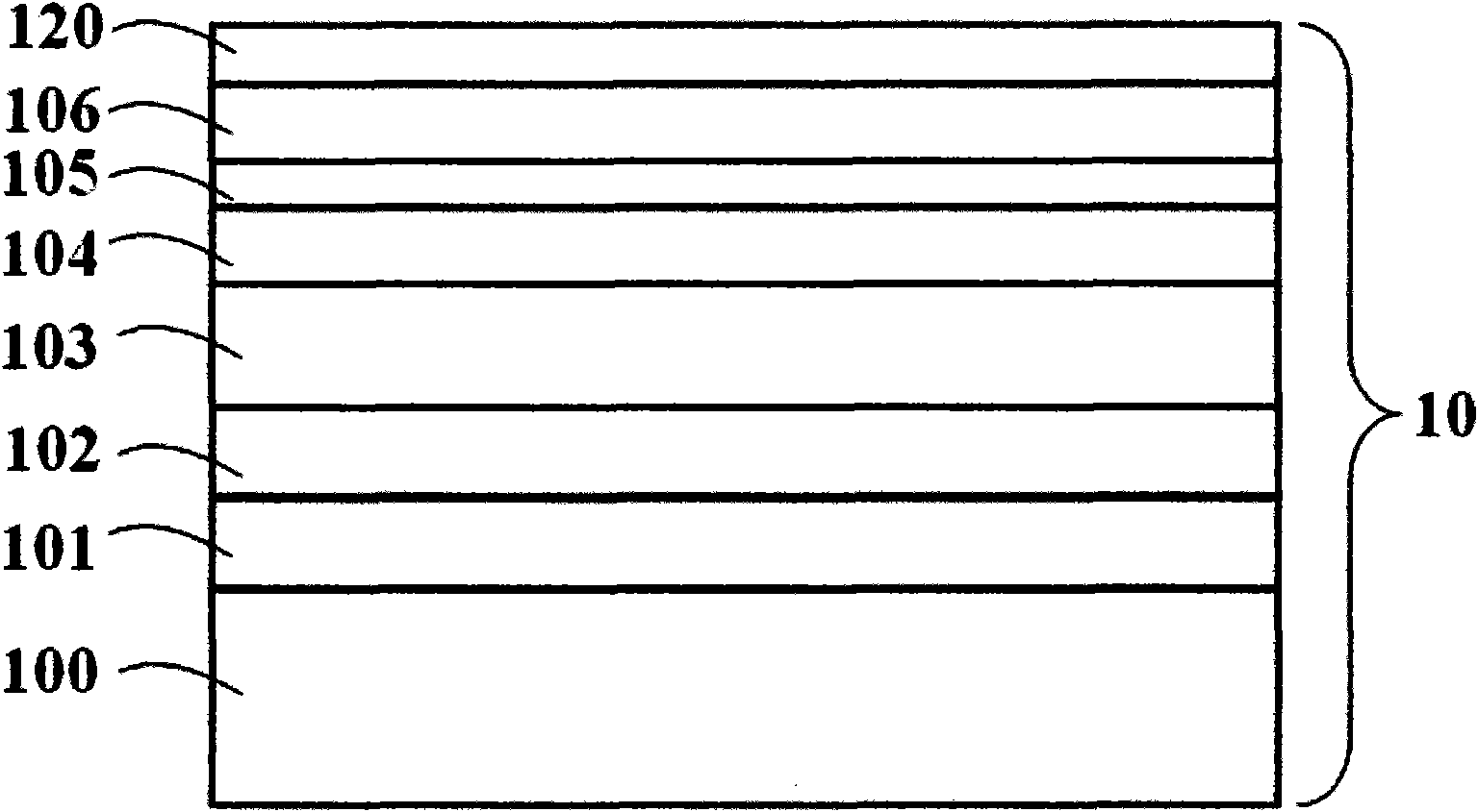
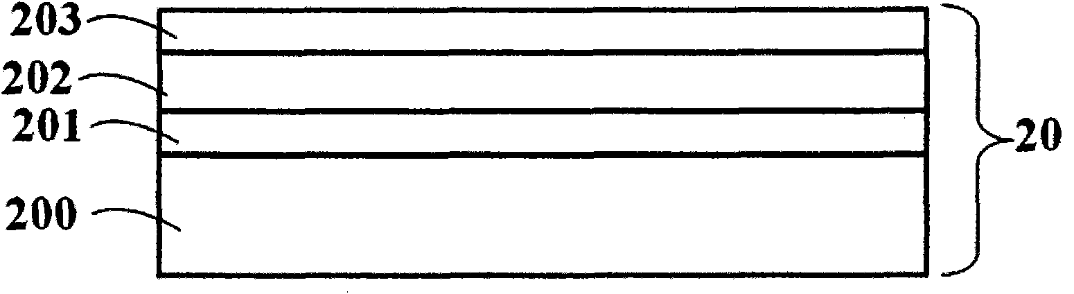
[0047] Such as figure 1 A schematic cross-sectional view of a gallium nitride-based light-emitting diode structure with an introductory roughened nitrogen polar surface shown, the structure comprising: a sapphire substrate 100; a buffer layer 101 formed on the sapphire substrate 100; a u-GaN layer 102 is formed on the buffer layer 101; the n-GaN layer 103 is formed on the buffer layer 102; the multi-quantum well active layer 104 is formed on a part of the n-GaN layer 103; the p-AlGaN confinement layer 105 is formed on On the multi-quantum well active layer 104; the p-GaN layer 106 is formed on the p-AlGaN confinement layer 105; the ITO transparent conductive layer 120 is formed on the p-GaN layer 106; the bonding layer 203 is formed on the ITO layer 120 Above part of the area, its material is In 0.2 Ga 0.8 N; the nitrogen polar surface roughened n-Ga...


PUM

PropertyMeasurementUnit
thicknessaaaaaaaaaa

Abstract

The invention discloses an introduction-type roughening nitrogen polar surface gallium nitride based light-emitting diode and a manufacturing method thereof. Based on the chip structure of the conventional allium nitride based light-emitting diode, a nitrogen polar surface gallium nitride epitaxial layer with a roughened surface is introduced through diffusion bonding and substrate removal, thereby solving a series of problems and limitations in the existing epitaxial surface roughening technology by using a chemical wet method, improving the light extraction efficiency of the light-emitting diode, keeping the original electrical properties of a chip unchanged, and obtaining the manufacturing yield almost same as the conventional gallium nitride based light-emitting diode.

Description

technical field [0001] The invention relates to a gallium nitride-based light-emitting diode and a manufacturing method thereof, more specifically a gallium nitride-based light-emitting diode combined with an introduced roughened nitrogen polar surface epitaxial layer and a manufacturing method thereof, which can improve the nitriding Light extraction efficiency of gallium-based light-emitting diode chips. Background technique [0002] In recent years, the development of semiconductor lighting technology represented by gallium nitride-based wide-bandgap semiconductor materials has attracted worldwide attention. With the continuous improvement of epitaxy and chip process technology, the luminous efficiency of gallium nitride-based light-emitting diodes has been continuously improved. However, in order to popularize semiconductor lighting in a real sense, it still needs to continue to improve on the existing level of light efficiency. The light efficiency of light-emitting d...

Claims


Application Information

Patent Timeline
Patent Type & Authority Applications(China)
IPC IPC(8): H01L33/20H01L33/22
Inventor 潘群峰吴志强林雪娇
Owner XIAMEN SANAN OPTOELECTRONICS TECH CO LTD
Why Eureka
Try Eureka