Macrolattice mismatch epitaxial material buffer layer structure containing superlattice isolated layer and preparation thereof

A lattice mismatch and epitaxial material technology, applied in semiconductor/solid-state device manufacturing, electrical components, circuits, etc., can solve the problem that the buffer layer has no special function, and achieve improved material properties, reduced thickness, and easy operation control. Effect

Active Publication Date: 2010-08-25
SHANGHAI INST OF MICROSYSTEM & INFORMATION TECH CHINESE ACAD OF SCI
View PDF0 Cites 21 Cited by
  • Summary
  • Abstract
  • Description
  • Claims
  • Application Information

AI Technical Summary

Problems solved by technology

However, the buffer layer has no special effect on optics and electricity, so it is hoped t...

Method used


Image

  • Macrolattice mismatch epitaxial material buffer layer structure containing superlattice isolated layer and preparation thereof
  • Macrolattice mismatch epitaxial material buffer layer structure containing superlattice isolated layer and preparation thereof
  • Macrolattice mismatch epitaxial material buffer layer structure containing superlattice isolated layer and preparation thereof

Examples


Embodiment 1

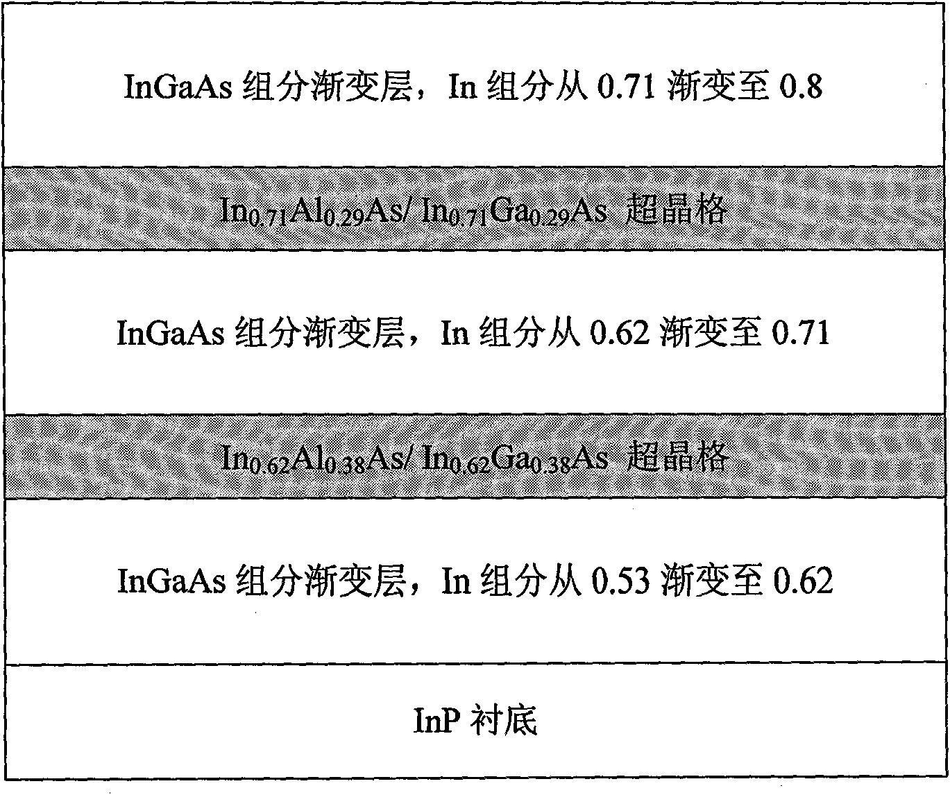
[0045] For epitaxy of In on InP substrates 0.8 Ga 0.2 Buffer Layer Structure of InAlAs / InGaAs Superlattice Isolation Layer Inserted in Continuous Gradient Buffer Layer of As Large Lattice Mismatched Material

[0046] (1) It is necessary to epitaxially high-quality In on the InP substrate .8 Ga 0.2 As large lattice mismatch material, the required growth thickness is thicker than the critical thickness, and it needs to be grown in the epitaxial In .8 Ga 0.2 The buffer layer was grown before the As material;

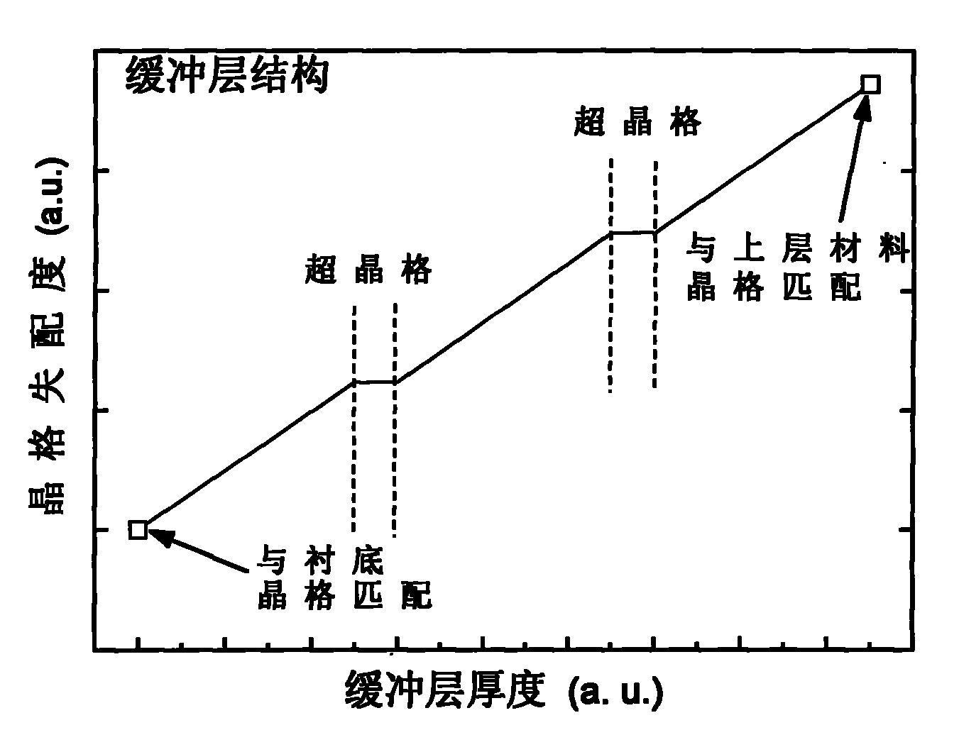
[0047] (2) The material is grown by the conventional molecular beam epitaxy method. The schematic diagram of the In composition change in the buffer layer structure is shown in Figure 2, and the schematic diagram of the buffer layer structure is shown in Figure 3. x Ga 1-x Two layers of InAlAs / InGaAs superlattice are inserted into the buffer layer with graded As composition, and the buffer layer is divided into 3 parts on average;

[0048] (3) Before the formal growt...

Embodiment 2

[0056] Buffer layer structure with InGaSb / InAlSb superlattice isolation layer inserted in InGaSb composition continuously graded buffer layer for epitaxial InSb large lattice mismatch material on GaSb substrate

[0057] (1) In order to epitaxially thicker high-quality InSb large lattice mismatch materials on GaSb substrates, it is necessary to grow In before epitaxial InSb materials. x Ga 1-x Sb buffer layer structure (0

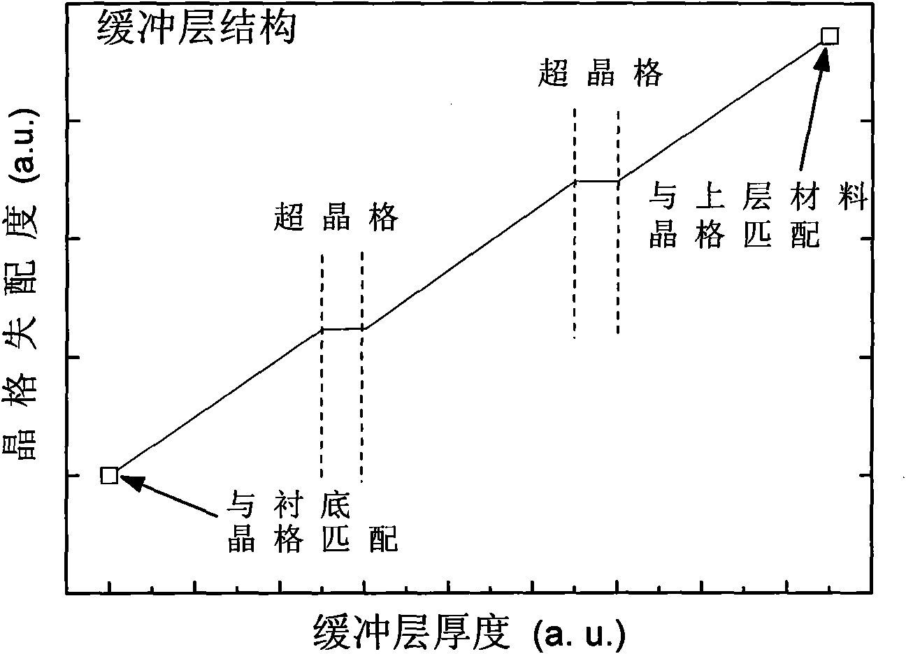
[0058] (2) The conventional molecular beam epitaxy method is used to grow the material. The schematic diagram of the composition change of In in the buffer layer structure is shown in Fig. 4, and the schematic diagram of the buffer layer structure is shown in Fig. 5. In the In x Ga 1-x 2 layers of InGaSbAs / InAlSb superlattice are inserted into the buffer layer with graded Sb composition, and the buffer layer is divided into 3 parts on average;

[0059] (3) Determine the beam source furnace temperature when growing GaSb and InSb on the GaSb substrate...


PUM

PropertyMeasurementUnit
Thicknessaaaaaaaaaa

Abstract

The invention relates to a macrolattice mismatch epitaxial material buffer layer structure containing a superlattice isolated layer and preparation thereof. N layers of strain-free superlattice isolated layer materials are inserted in a component gradual change buffer layer, wherein n is a natural number and is not smaller than 1 and not larger than 5. The preparation process comprises the following steps of: firstly, determining the parameters of growth temperature, beam source furnace temperature and other parameters; and then sequentially and alternately growing buffer layers with gradually increased strain capacities and strain-free superlattice isolated layer materials on a substrate by adopting a molecular beam epitaxy method until finishing the growth of a buffer layer reaching an expected strain capacity. The material contains the superlattice isolated layer and can ensure that relaxation can quickly and effectively occur to a macrolattice mismatch epitaxial material to release stress in the buffer layer so as to reduce the dislocation density of the epitaxial material on the buffer layer. Moreover, the uninterrupted growth of the material is carried out by adopting a conventional molecular beam epitaxy method, thus the invention has the advantages of easy control of operations, low cost, environmental protection, and the like.

Description

technical field [0001] The invention belongs to the field of large lattice mismatch epitaxial material buffer layer structure and preparation thereof, in particular to a large lattice mismatch epitaxial material buffer layer structure including a superlattice isolation layer and its preparation. Background technique [0002] With the development of semiconductor energy band engineering and the advancement of material epitaxy technology, more and more attention has been paid to heteroepitaxy materials with a lattice mismatch with the substrate. When a lattice-mismatched material is epitaxially grown on a substrate, when the mismatched epitaxial layer is sufficiently thin, the lattice constant of the epitaxial layer will be compatible with the lattice of the substrate under the action of the deformation energy generated by the lattice mismatch. The constants are kept consistent to avoid dislocations. However, when the epitaxial thickness exceeds a certain thickness (called cr...

Claims


Application Information

Patent Timeline
IPC IPC(8): H01L21/203
Inventor 顾溢张永刚
Owner SHANGHAI INST OF MICROSYSTEM & INFORMATION TECH CHINESE ACAD OF SCI
Why Eureka
Try Eureka